Table of Contents
Design teams and purchasing managers are increasingly asked to move new products to lead-free PCB assembly, but the practical impact on materials, processes, and reliability is not always clear.
Switching from traditional leaded solder to lead-free alloys affects everything from solder paste selection and reflow profiles to PCB laminates and through-hole soldering methods.
This article explains what lead-free PCB assembly really means in the context of SMT and through-hole projects.
We will walk through the key regulations behind lead-free manufacturing, commonly used solder alloys and PCB materials, how SMT and THT processes are affected, and what design and DFM points engineers should consider before moving a board into lead-free production.
By the end, you should have a clearer, practical understanding of how lead-free assembly impacts your PCB designs, manufacturing choices, and long‑term product reliability.
What Is Lead-Free PCB Assembly?
Basic Definition and Background
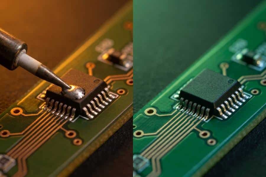
Lead-free PCB assembly is the process of soldering electronic components onto printed circuit boards using solders that do not contain intentionally added lead, typically to meet RoHS and similar environmental regulations.
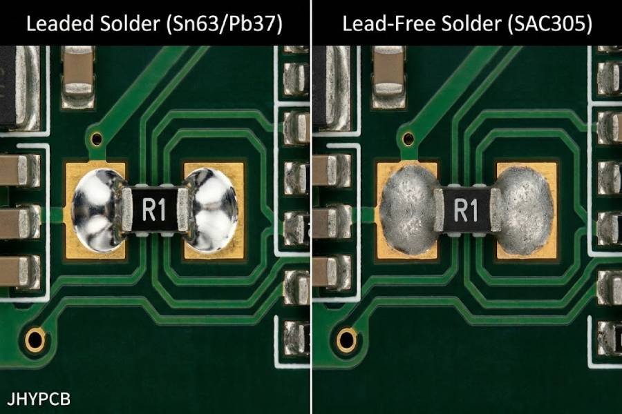
Instead of traditional tin–lead alloys such as Sn63/Pb37, manufacturers use lead-free alloys based on combinations of tin, silver, and copper (and sometimes other elements), which melt at higher temperatures and have different wetting and reliability characteristics.
For many years, lead-based solder was the default choice because it offered a relatively low melting point, good wetting, and stable mechanical properties.
As global electronics regulations tightened, especially in markets such as the European Union, lead in solders became a restricted substance, driving the industry toward lead-free PCB assembly for a growing share of products.
Regulatory Drivers: RoHS and Other Standards
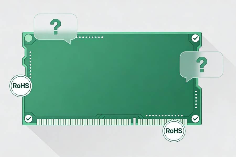
The most widely recognized driver behind lead-free PCB assembly is the Restriction of Hazardous Substances (RoHS) directive, initially introduced in the European Union and now reflected in many global market requirements.
RoHS typically limits the maximum allowable concentration of lead and several other hazardous substances in homogeneous materials, which means PCB finishes, solder alloys, and components must all be selected and controlled to stay within those limits.
Beyond RoHS, other regulations and customer specifications often reference lead-free and halogen-free materials, environmental reporting, and documentation of compliance.
As a result, lead-free PCB assembly is no longer just a technical choice about solder; it is a broader manufacturing and supply chain requirement that affects material selection, process control, and long‑term product strategy for many OEMs.
Lead-Free Solder Alloys and Materials
Common Lead-Free Solder Alloys for SMT and THT
In practice, moving to lead-free PCB assembly largely comes down to working with different solder alloys and understanding how they behave.
The most widely used family of lead-free solders is based on tin with small additions of silver and copper, such as SAC305 (approximately 96.5% Sn, 3.0% Ag, 0.5% Cu), which is common in both SMT reflow and many through-hole applications.
Compared to traditional Sn63/Pb37 solder, these lead-free alloys have higher melting points and require higher peak reflow temperatures, which changes the thermal stress experienced by the PCB, components, and solder joints.
In wave soldering or selective soldering, manufacturers may use lead-free alloys that are specifically tuned for pot stability, dross generation, wetting behavior, and long‑term mechanical performance.
Because of these differences, planning an SMT or THT project for lead-free production is not just a matter of “swapping in another solder.”
Engineers and manufacturing teams need to think about which alloy family to use, which assembly methods it supports, what reflow or soldering temperature window it requires, and how those choices affect reliability.
PCB Laminates and Surface Finishes in Lead-Free Assembly
The PCB material stack‑up and surface finish also play a bigger role under lead-free conditions.
Because reflow and wave solder temperatures are higher, properties such as glass transition temperature (Tg), decomposition temperature (Td), resistance to delamination, and performance under repeated thermal cycles all become more critical.
Common finishes like ENIG (electroless nickel immersion gold), OSP (organic solderability preservative), and immersion tin are still widely used in lead-free PCB assembly, but their impact on solderability, appearance, and shelf life is more pronounced.
For example, OSP can require tighter process control and storage conditions at higher temperatures, while ENIG often offers a more forgiving soldering window and stable performance for many high‑reliability lead-free designs.
Selecting materials with lead-free assembly in mind—rather than treating it as an afterthought—helps reduce issues such as pad lifting, board warpage, or poor wetting that might not have appeared in a leaded process.
Component and BOM Considerations
To achieve truly RoHS-compliant PCB assembly, it is not enough to change only the solder and PCB materials; every component in the BOM must also be compatible with lead-free processes.
This includes both compliance from a substance perspective (for example, lead-free finishes on leads and internal terminations) and the ability of each component package to tolerate higher reflow temperatures and thermal stress.
In day‑to‑day work, engineering and purchasing teams commonly verify component lead-free / RoHS status with suppliers, maintain clear coding for compliant parts, and identify any legacy components that need lead-free equivalents before a design is released to production.
Handled well, this upfront BOM work can significantly reduce trial‑build issues such as non‑solderable terminations, cracking, or delays caused by incomplete documentation in lead-free projects.
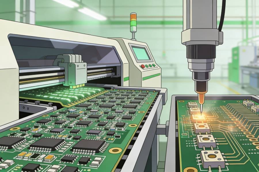
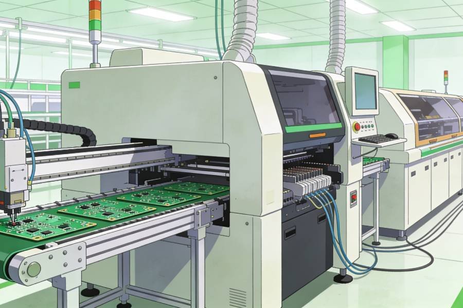
How Lead-Free Affects the SMT Assembly Process
Lead-Free Solder Paste Printing and Handling
In surface-mount technology (SMT), the move to lead-free PCB assembly starts with solder paste.
Lead-free pastes typically use SAC‑type alloys and have different viscosity, wetting behavior, and temperature requirements compared to traditional tin–lead formulations, which means print parameters and handling practices often need to be retuned.
Stencil design, squeegee speed and pressure, snap‑off distance, and environmental conditions all play a role in how consistently lead-free solder paste is deposited.
Because the process window can be narrower, maintaining stable paste temperature, humidity, and open time is especially important to avoid slumping, poor release, or insufficient solder on fine‑pitch pads.
Pick-and-Place for Lead-Free Projects
At first glance, the pick‑and‑place step looks almost unchanged when you switch to lead-free SMT assembly.
Machines still place components based on the same coordinates and vision data, but the higher reflow temperatures and different solder behavior make placement accuracy and coplanarity more critical for yield.
Components that were marginal in a leaded process—for example, slightly warped packages or boards—may cause more noticeable defects under lead-free conditions, such as open joints or uneven wetting.
As a result, many manufacturers tighten their process controls around placement, board support, and panel design when running lead-free production, especially for fine‑pitch ICs and dense BGA layouts.
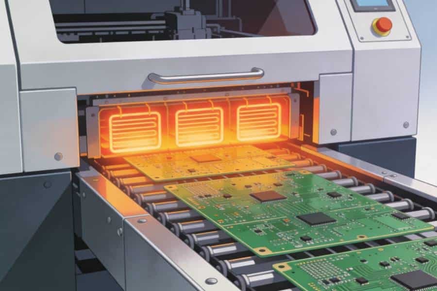
Reflow Profiles for Lead-Free vs. Traditional Alloys
Reflow soldering is where most of the practical differences between leaded and lead-free SMT assembly become obvious.
Lead-free solder alloys generally require higher peak temperatures and carefully controlled soak and cooling segments, which increases the thermal stress applied to the PCB, components, and solder joints.
A typical lead-free reflow profile will have a longer time above liquidus and a higher peak temperature window than a Sn63/Pb37 profile, so profile development and verification are not optional steps—they are central to achieving reliable results.
Engineers need to balance complete solder reflow and wetting against the risk of board warpage, delamination, package damage, and cosmetic issues such as duller joint appearance, which is common in lead-free PCB assembly but does not necessarily indicate a defective joint.
Lead-Free Through-Hole and Mixed Technology Assembly
Lead-Free Wave Soldering for Through-Hole Components
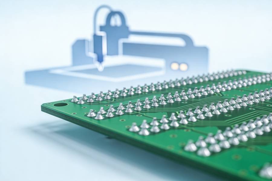
Through-hole technology (THT) is still widely used for connectors, transformers, large capacitors, and other components that need strong mechanical support or must handle higher currents.
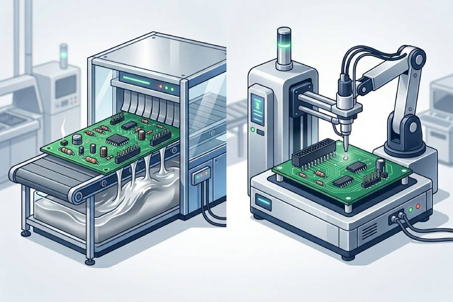
In lead-free PCB assembly, these parts are often soldered using wave soldering, where the underside of the PCB is passed over a controlled “wave” of molten lead-free solder at a higher pot temperature than in traditional tin–lead processes.
Typical lead-free wave soldering runs with solder pot temperatures in the 245–270 °C range and requires careful control of preheat, flux, conveyor speed, and contact (dwell) time to achieve reliable hole fill without damaging the PCB or components.
Because the entire underside of the board is exposed to the wave, design practices such as using pallets, thieving pads, and appropriate lead protrusion become more important to minimize bridging, shadowing, and other THT defects under lead-free conditions.
Selective Soldering and Manual Soldering in Lead-Free THT
As mixed-technology PCBs have become more common, selective soldering has become a key tool for lead-free through-hole assembly.
Instead of exposing the whole board to a full wave, selective soldering uses programmable nozzles to apply molten lead-free solder only to specific pins or areas, which is especially useful when dense SMT components sit close to THT pins that still require robust solder joints.
Selective soldering is usually slower and more complex to set up than traditional wave soldering, but it offers better control of thermal exposure, lower risk of disturbing nearby SMT joints, and more flexibility for complex mixed-technology layouts.
For special cases, manual lead-free soldering is still used—for example, rework, low-volume assemblies, or unique connectors—but it requires appropriate tools, tip temperatures, and operator training to avoid cold joints or component damage at higher lead-free soldering temperatures.
Combining Lead-Free SMT and THT on One Board
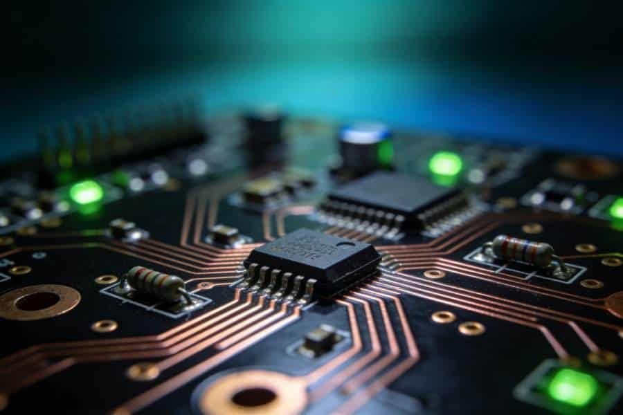
Most real‑world designs today are mixed-technology PCBs, combining SMT for dense circuitry with THT for mechanically robust or high‑power components.
In a lead-free PCB assembly flow, SMT components are typically placed and reflowed first, followed by wave soldering, selective soldering, or manual soldering of the remaining through-hole parts, using fixtures or pallets where needed to protect sensitive SMT areas from the solder wave.
This mixed approach allows designers to get the best of both worlds: compact, high‑speed SMT circuits and durable THT terminations for connectors and high‑stress parts, all within a lead-free, RoHS-compliant manufacturing framework.
However, it also means that layout, panel design, process choice (wave vs. selective), and assembly sequencing must be planned together with the factory to ensure that both SMT and through-hole joints can meet reliability targets under lead-free conditions.
Benefits and Challenges of Lead-Free PCB Assembly
Environmental and Compliance Benefits
The most obvious advantage of lead-free PCB assembly is that it supports more environmentally responsible electronics manufacturing and helps reduce hazardous substances in the waste stream.
By replacing traditional leaded solders and finishes with RoHS-compliant materials, manufacturers lower the amount of lead that can end up in landfills, incineration systems, and recycling processes, which ultimately reduces long‑term risks to soil, water, and human health.
For companies shipping into markets such as the European Union and other regions that follow similar regulations, using lead-free, RoHS-compliant PCB assembly is no longer optional—it is a requirement for maintaining market access and avoiding compliance issues.
Adopting lead-free processes also sends a clear signal to customers and partners that the business takes sustainability and regulatory responsibilities seriously, which can be a differentiator in sectors that care deeply about environmental performance.
Technical Challenges: Higher Temperatures and Reliability Risks
The main trade‑offs with lead-free PCB assembly come from the higher processing temperatures and the different behavior of lead-free solder joints.
Higher peak reflow and wave solder temperatures place more stress on PCB laminates, copper structures, and component packages, which can increase the risk of warpage, delamination, pad lifting, or internal damage if materials and profiles are not chosen carefully.
On the joint level, lead-free solders tend to form different microstructures than tin–lead alloys and can be more prone to issues like brittle fracture under certain loading or thermal cycling conditions.
This does not mean that lead-free assemblies are inherently unreliable, but it does mean that material selection, profile tuning, and reliability testing become more important, especially for harsh environments such as automotive, industrial, or aerospace electronics.
Best Practices to Improve Lead-Free Assembly Yield
In well‑run factories, many of the challenges associated with lead-free PCB assembly are managed through process engineering and upfront design choices.
Good practice typically includes selecting laminates and finishes rated for lead-free temperatures, developing robust reflow and wave profiles, controlling solder paste and flux processes tightly, and using AOI and electrical testing to catch defects before boards leave the line.
From the design side, engineers can support higher yields by following DFM guidelines for pad design, thermal reliefs, stencil apertures, and mixed-technology layouts that are compatible with lead-free soldering.
When material choices, PCB layout, and assembly processes are aligned for lead-free production, most organizations find that they can meet both regulatory and reliability requirements without sacrificing product performance.
Design and DFM Tips for Lead-Free SMT and THT Projects
Layout and Pad Design Considerations
Lead-free PCB assembly puts a bit more pressure on layout and pad design because the process window can be narrower and the solder behavior is different from tin–lead.
Pad sizes, solder mask clearances, stencil apertures, and the use of thermal reliefs all influence how lead-free solder wets the pads, how likely tombstoning or bridging will be, and how robust the joints will be under thermal cycling.
For fine‑pitch SMT components, keeping a consistent pad-to-aperture ratio and avoiding unnecessary asymmetry between pads helps reduce imbalanced forces during reflow that can lift small parts.
In THT areas, hole size, annular ring width, and lead protrusion need to account for lead-free wave or selective soldering conditions so that barrels fill properly without excessive solder spikes or voids.
Thermal Management and Board Stack-Up
Because lead-free reflow and wave soldering run hotter, thermal management and PCB stack‑up decisions have a stronger impact on both assembly and field reliability.
Copper thickness, plane distribution, thermal vias, and local copper density all affect how evenly heat flows through the board during soldering and how well the design handles operating temperature once the product is in use.
Dense copper areas around pads can act as heat sinks and make it harder for certain joints to reach the correct temperature, which can be more problematic with lead-free solder’s higher melting point.
Thoughtful use of thermal spokes, balanced copper on opposite layers, and attention to where high‑power components sit in the stack‑up can help avoid cold joints during assembly and reduce thermo‑mechanical stress on solder joints over the product’s lifetime.
DFM Review Before Lead-Free Production
One of the most effective ways to improve outcomes in lead-free PCB assembly is to run a proper DFM review with the manufacturing partner before the design is released to production.
A good DFM check for lead-free projects looks at things like pad geometry, stencil design, component spacing, test‑point access, panelization, and whether the chosen materials and finishes are appropriate for the planned soldering processes.
For mixed-technology boards, the review should also confirm how SMT and THT steps will be sequenced, whether wave or selective soldering is planned, and whether any keep‑out or pallet requirements need to be reflected in the design.
Catching these details early saves time and cost later by reducing trial builds, rework, and last‑minute design changes that are much harder to make once a lead-free product is already in production.
How to Choose a Lead-Free PCB Assembly Partner
Key Capabilities to Look For in SMT and THT
Choosing the right partner for lead-free PCB assembly is as much about process capability as it is about certifications and pricing.
A good manufacturer should be able to demonstrate solid experience with lead-free SMT and through-hole assembly, including reflow profiling, wave or selective soldering, and inspection methods that are tuned for RoHS-compliant products.
On the SMT side, look for evidence of stable lead-free production on fine‑pitch devices, BGAs, and high‑density layouts, ideally backed by AOI and X‑ray where appropriate.
For THT and mixed-technology boards, your partner should be comfortable with lead-free wave and selective soldering, fixture design, and process development for connectors and other mechanically stressed components.
Questions to Ask About Process Control and RoHS Compliance
When evaluating potential lead-free PCB assembly partners, the questions you ask can reveal a lot about how mature their processes really are.
It is worth asking how they develop and verify lead-free reflow and wave profiles, what kinds of process controls and SPC they use, and how they handle AOI, electrical testing, and final inspection for RoHS-compliant assemblies.
On the compliance side, you should also understand how they manage RoHS documentation, material declarations, and traceability for solder, PCB laminates, surface finishes, and components.
Clear answers in these areas not only help you meet regulatory expectations, they also reduce the risk of surprises later if customers or auditors ask for proof of lead-free and RoHS compliance.
When to Consider Turnkey Lead-Free Assembly Services
In many projects, especially when schedules are tight or teams are small, turnkey lead-free PCB assembly can simplify both logistics and compliance.
Under a turnkey model, the assembly partner sources PCBs and components, manages the supply chain for lead-free and RoHS-compliant materials, and delivers fully assembled boards, which can reduce coordination work for the OEM.
Turnkey lead-free assembly is particularly attractive when a design uses many components with specific RoHS or temperature requirements, or when the organization does not want to manage multiple suppliers and material declarations on its own.
Whether you choose turnkey or consigned models, the key is to work with a lead-free PCB assembly partner that treats process control and compliance as core strengths rather than add‑ons.
Conclusion
Lead-free PCB assembly is no longer a niche option—it is the standard for many RoHS-compliant electronic products and markets around the world.
Moving from traditional leaded processes to lead-free soldering affects materials, SMT and through-hole assembly parameters, reliability expectations, and how design and manufacturing teams work together.
By understanding the basics of lead-free solder alloys, PCB materials, reflow and wave profiles, and mixed-technology process planning, engineers and buyers can make more informed decisions and avoid many common pitfalls.
A structured DFM review and the right lead-free PCB assembly partner help turn those decisions into stable production, whether the goal is a small prototype run or ongoing volume manufacturing.
If you are planning a new lead-free SMT or through-hole project and need support with RoHS-compliant PCB assembly, it is worth discussing your design, materials, and reliability goals early with a manufacturer that has proven experience in lead-free production.