

Custom Flex PCB:Tailored Solutions for Your Applications
In today’s rapidly evolving electronics landscape, flexibility and adaptability are paramount. Custom flex PCBs offer a tailored solution that combines
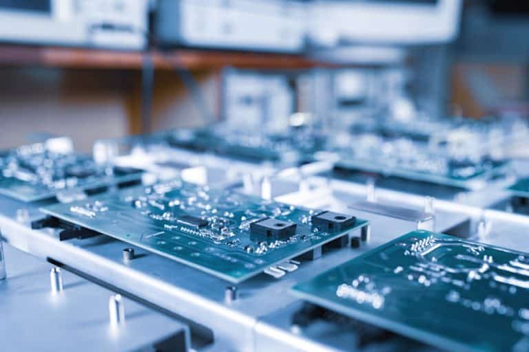
Custom PCB Manufacturing in Germany – Fast Prototype & Assembly Services
Looking for reliable custom PCB manufacturing services in Germany? PCBELEC provides fast PCB prototyping, high-quality mass production, and turnkey assembly
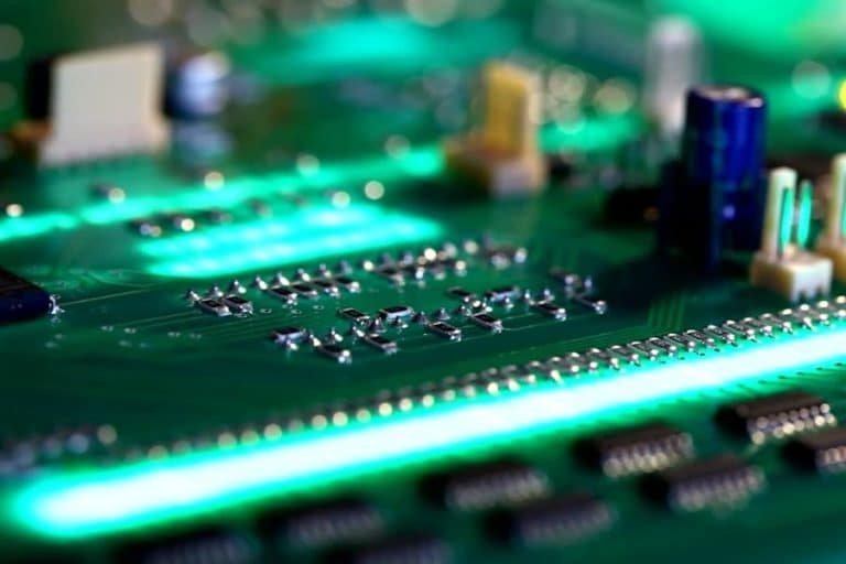
Custom PCB Fabrication in China – Prototyping & Mass Production
At PCBELEC, a leading custom PCB manufacturer in China, we provide reliable solutions for all your prototyping, mass production, and
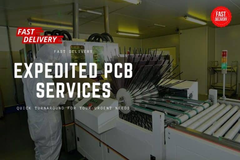
Expedited PCB Services – Quick Turnaround for Your Urgent Needs
Need PCB prototypes, production runs or assemblies delivered fast? PCBELEC’s expedited PCB services provide rapid turnaround times to meet your

Rapid PCB Prototyping and Production – The Keys to Accelerating Your Product Launch
In today’s fast-paced product development cycles, rapid PCB prototyping and accelerated production services are crucial for achieving first-mover advantage. This

Aluminum PCB Prototype: The Ultimate Guide for Engineers and Designers
Aluminum PCB prototypes offer superior performance and reliability compared to traditional FR4 PCB prototypes. This blog post provides you with
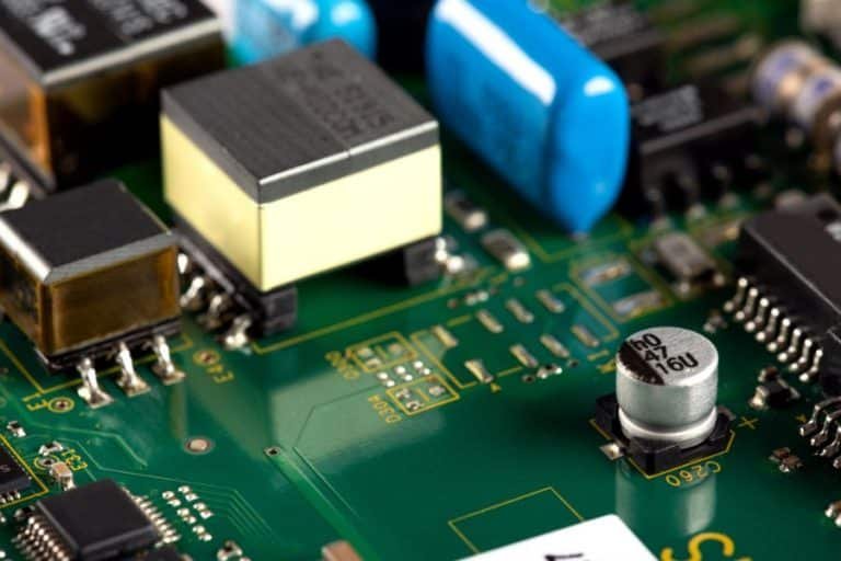
Fast and Reliable PCB Prototyping with PCBELEC in Australia
Looking for reliable PCB prototype services in Australia? Look no further! PCBELEC offers high-quality manufacturing processes, competitive pricing, and streamlined

A Complete Guide on PCB Drilling Process
This definitive guide covers all PCB drilling process fundamentals – understanding different hole types like plated through holes (PTHs), preparation

Rohs Compliant PCBs: A Complete Guide to RoHS Standards for Printed Circuit Boards
A complete guide to RoHS standards for printed circuit board manufacturing, assembly and testing. Learn about restricted substances, compliance benefits,

What is the Difference Between PTH and Via in PCBs?
Understanding the key differences between PTH and via is essential for optimizing PCB design and manufacturing. This article defines PTH

What is Backdrilling of Vias and Why it Matters for PCBs
With the exponential rise of high-frequency applications, backdrilled vias are increasingly critical for minimizing via stub impedance on PCBs. As
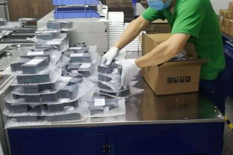
Navigating The PCB Manufacturing Process Part 5: Testing, V-cut, QC, And Shipping
Explore the intricate journey of double-layer PCB manufacturing at PCBELEC, from routing to shipping. Witness the precision of processes like

Navigating The PCB Manufacturing Process Part 4: Solder Mask, Silkscreen, Surface Finish
We have now covered initial PCB production processes – substrate preparation, imaging, plating, etching to form circuitry. The board is

Navigating The PCB Manufacturing Process Part 3: Pattern And AOI
We have covered initial PCB production steps – milling, foil lamination, drilling. Now we detail processes to transform base material
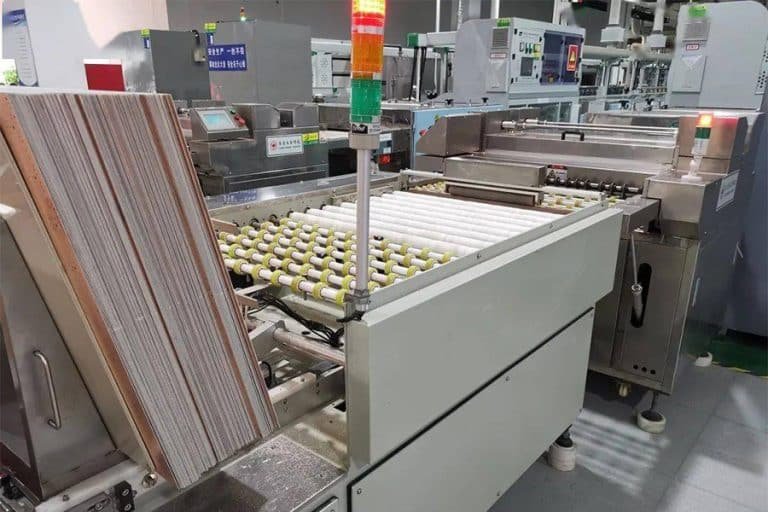
Navigating The PCB Manufacturing Process Part 2: Copper Plating, Routing
In our PCB manufacturing process deep dive, we explored lamination, exposure, and development steps that transfer circuit layouts onto boards.

Navigating the PCB Manufacturing Process Part 1: Unveiling MI, Cutting, and Drilling
Dive into the world of PCB manufacturing with our comprehensive guide, focusing on three crucial stages: Manufacturing Instruction (MI), Material
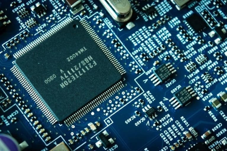
Fast Prototype PCB Manufacturing Services in Canada by PCBELEC
PCBELEC offers fast PCB prototype and reliable rapid PCB prototyping services in Canada for startups and enterprises, manufacturing boards with
UK PCB Prototype Manufacturing: Fast, Affordable, and High-Quality
As a leading China PCB manufacturer, we specialize in fast turnaround prototype PCB manufacturing and assembly for UK companies. Leverage