
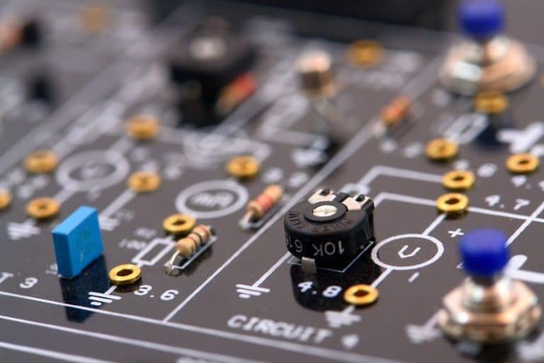
Rapid PCB Prototyping Services: A Comprehensive Introduction
Rapid PCB prototyping allows functional validation of printed circuit board layouts within 24-120 hours. Rapid PCB prototyping services enable engineers
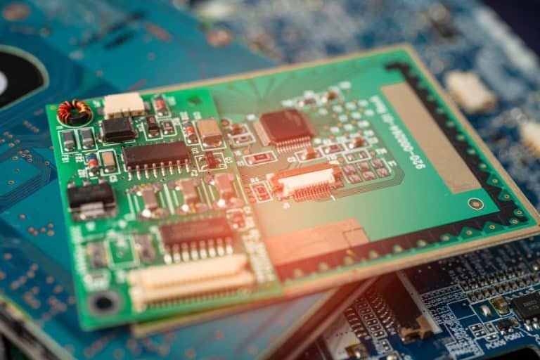
The Benefits of Using Double Sided PCBs
Double sided PCBs unlock more layout space, reduce layers, improve signal integrity & offer flexible arrangements. For rapid prototyping, dual

Gerber Files for PCB Prototyping – A Comprehensive Guide
A definitive guide covering everything about Gerber files – from formats, layer types, naming conventions to quality checks and transfer

Key Differences Between Prototype and Production PCBs Explained
What key differences should you keep in mind between prototype and production printed circuit boards? This article explains lead times,
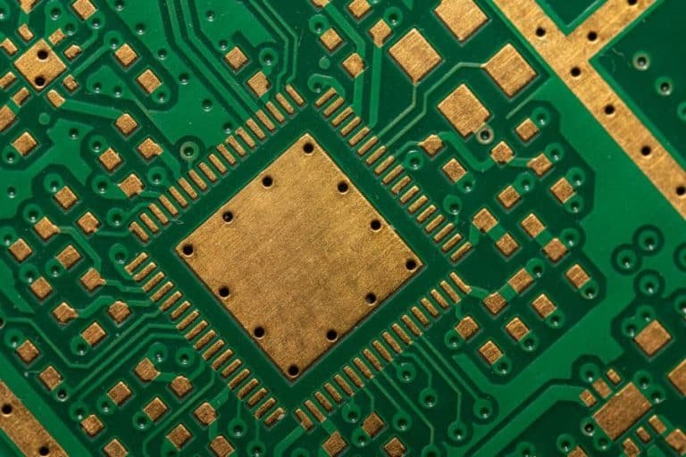
What is a Blank PCB
A blank PCB, also known as a bare PCB, refers to a printed circuit board that serves as a base

Introduction to Semi-Flex PCBs: Bridging Rigid and Flex PCBs
Semi-flex PCBs offer the perfect balance between rigid and fully flexible PCBs. With partial flex and partial rigidity, they provide

Fast Prototype PCB Services for US Customers
Looking for fast turnaround on prototype PCBs without the high costs? PCBELEC, a leading PCB manufacturer in China, provides rapid

How to Choose the Best LED Grow Light PCB for Indoor Gardening
Selecting the right LED grow light PCB is crucial for thriving indoor gardens. This guide covers light spectrum, power efficiency,
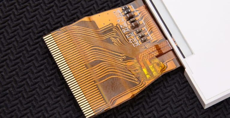
The Ultimate Guide to Flexible PCB Manufacturing and Assembly
As a premier flexible PCB manufacturer in China, PCBELEC has extensive expertise in fabricating and assembling high-quality flex circuits. In

Choosing the Right PCB Material for Your Prototype: A Comprehensive Guide
Discover the best PCB materials for your prototyping needs with our comprehensive guide. From FR-4 to metal core and Rogers

Why Should You Consider PCB Prototyping for Your Next Project?
PCBELEC offers PCB prototyping services that provide cost-effective, high-quality PCBs, faster turnaround times, and the ability to test and make

The Ultimate Guide to PCB Prototype Manufacturing: Everything You Need to Know
Looking for a reliable PCB prototype manufacturer? Look no further than PCBELEC. With years of experience and a commitment to

Exploring the Benefits and Challenges of PCB Prototype Manufacturing in China
Learn the advantages of China’s PCB prototype manufacturing, including cost savings and advanced technology, and how PCBELEC ensures high-quality prototypes
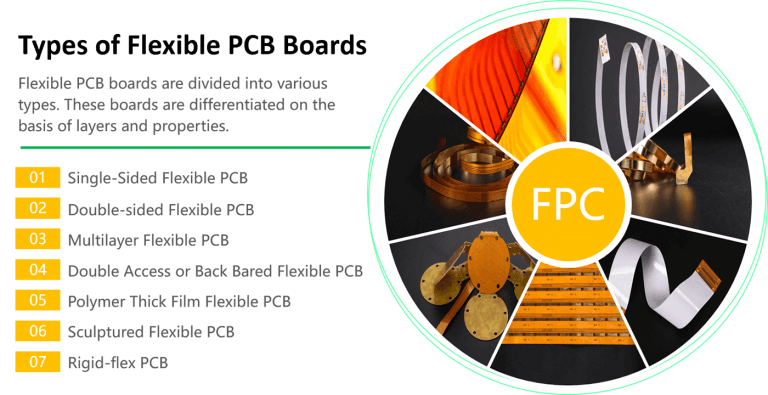
Types of Flexible Circuit Boards: The Ultimate Guide to Flex PCBs
Discover the six types of flexible circuit boards, from single-sided to rigid-flex, with key advantages and applications. Unlock innovative designs

How to Build a Multilayer PCB: A Comprehensive Guide
Learn how to build multilayer PCBs with this guide on stack-up design, manufacturing processes, IPC standards, and storage tips for
Why PCB Prototyping is Essential for Cost-Effective Design Success
PCB prototyping is a critical step in electronics design, enabling you to validate functionality, reduce costs, and accelerate time-to-market. Learn
Essential Requirements for Successful PCB Prototype Manufacturing in 2025
Learn the essential requirements for PCB prototype manufacturing, including file formats, design rules, layer stackup, and documentation. Optimize your prototyping
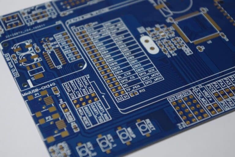
A Complete Guide to Ordering a PCB Prototype Service
Ordering a PCB prototype service? Our guide covers essential factors like materials, layers, and surface finishes, with practical tips to