
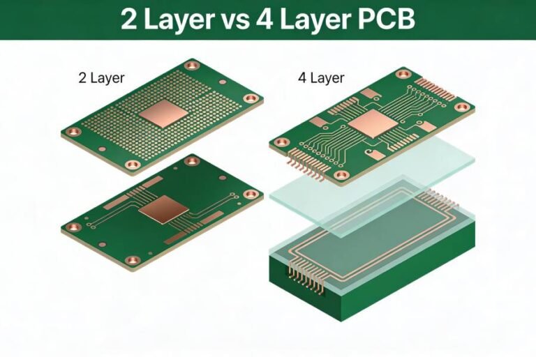
2 Layer vs 4 Layer PCB: Cost, EMI, and When to Upgrade
Not sure if your next board should be 2 or 4 layers? This guide compares structure, EMI, routing density, and
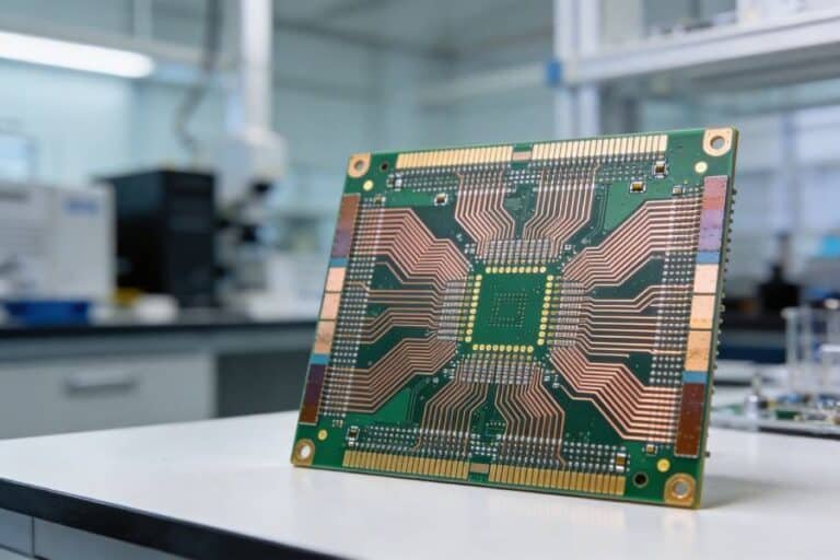
High‑Speed PCB Materials: FR‑4 vs Megtron 6 vs Rogers 4000 vs PTFE Compared
Choosing the right laminate is one of the most consequential decisions in any high‑speed PCB project. The wrong material can
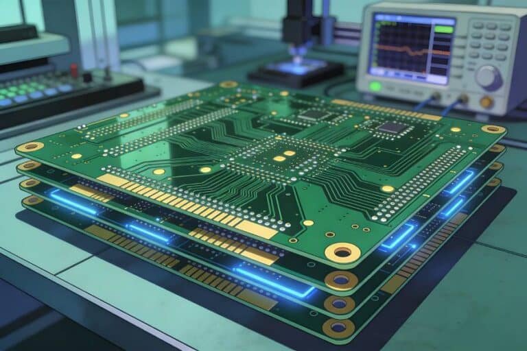
High‑Speed PCB Manufacturing Guide: From Stack‑Up and Materials to Reliable Fabrication
High‑speed PCB design does not end when the layout is finished. To achieve stable signal integrity at multi‑gigabit speeds, your

High Frequency PCB Prototype to Production: RF PCB Prototyping and Manufacturing Guide
Moving a high frequency PCB from prototype to production is very different from scaling a standard FR‑4 design. RF PCB

High Frequency PCB Cost: Key RF PCB Manufacturing Cost Factors and Optimization Tips
High frequency PCB cost is driven by much more than board size and layer count. Materials like Rogers and PTFE,

High Frequency PCBs for 5G Base Stations and Small Cells | Design & Manufacturing Tips
High frequency PCBs are at the core of 5G macro base stations and small cells, where Sub‑6 and mmWave signals

High Frequency PCB Material Selection for 5G, Radar and Satellite Applications
5G, radar, and satellite PCBs push into GHz and mmWave bands where material choice directly controls loss, phase stability, and

How to Choose High Frequency PCB Materials: Rogers, PTFE and High Performance FR4
Choosing the right high frequency PCB material is a balance between electrical performance, cost and manufacturability. This guide explains when

What Is High Frequency PCB? Definition, Materials & Applications
A high frequency PCB is a printed circuit board designed for RF and microwave signals, typically from hundreds of MHz

How to Panelize and Route Gold Finger PCBs for Better Yield and Reliability
Panelization and routing choices can make or break the yield and reliability of gold finger PCBs. This practical guide shows

Step-by-Step Guide to Gold Finger PCB Design & Manufacturing
This practical, step-by-step guide walks you through the entire process of a Gold Finger PCB, from defining application requirements and

How PCB Manufacturers Use TDR and Coupons to Verify Controlled Impedance
Specifying controlled impedance is only half the job – you also need to verify it. This article explains what PCB

How to Specify Controlled Impedance Requirements to Your PCB Manufacturer
Clear controlled impedance requirements can make the difference between a smooth PCB fabrication run and weeks of delays and redesigns.

Choosing the Right PCB Material for LED Applications: Top Selection Strategies
In LED applications, choosing the right PCB material is vital for heat dissipation and reliability. Learn why aluminum MCPCBs outperform
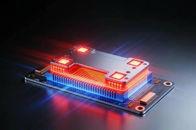
Thermal Management in LED PCB: How to Prevent Overheating (2026 Engineering Guide)
LED junction temperatures above 85°C cut lifespan by 50%+. This deep dive covers aluminum LED PCB thermal engineering: MCPCB dielectric

LED PCB Manufacturing Process: From Design to Assembly
LED PCB manufacturing transforms engineering files into reliable lighting modules through 10+ critical process steps. This guide details aluminum LED

How to Choose a Reliable LED PCB Manufacturer
Choosing the right LED PCB manufacturer directly affects the performance, lifetime and safety of your LED products. This guide explains

LED PCB Design Guide: Best Practices for Optimal Performance
Designing LED PCBs demands far more than applying standard PCB design rules. While conventional circuit boards prioritize electrical performance and