Table of Contents
Introduction to Multilayer PCB Fabrication
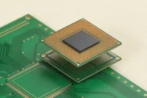
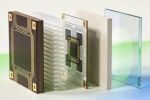
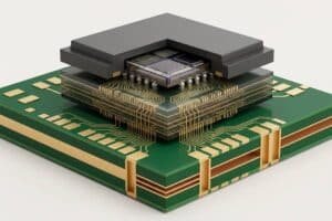
Multilayer PCBs are the backbone of modern electronics, enabling compact, high-performance devices. Unlike single-sided or double-sided PCBs, multilayer PCBs consist of three or more layers of conductive copper separated by insulating substrates, typically fiberglass and epoxy. This structure supports higher component density, improved signal integrity, and enhanced functionality, making them essential for applications like smartphones, medical devices, automotive systems, and 5G infrastructure.
The demand for multilayer PCBs has increased with the advancement of electronic technologies. A 2024 report by Market Research Future projects the global PCB market to grow at a CAGR of 4.3% from 2022 to 2030, with multilayer PCBs accounting for approximately 55-60% of the market in 2022, driven by their versatility. However, fabricating multilayer PCBs requires precision at every stage, particularly in layer alignment, where errors can lead to signal interference or circuit failure.
Multilayer PCB Market Share
The chart below illustrates the estimated market share of multilayer PCBs in the global PCB industry.

Why Layer Alignment Matters in Multilayer PCB Fabrication
Precise layer alignment is critical in multilayer PCB fabrication to ensure proper electrical connectivity. Each layer contains copper traces that must align within tolerances as tight as 0.001 inches (25.4 micrometers). Misalignment can cause short circuits, open circuits, or signal degradation, rendering the PCB unusable. In high-speed applications like 5G devices, misalignment can introduce interference, compromising performance. A 2024 IPC study estimates that alignment-related defects account for 15% of PCB manufacturing failures, leading to costly rework or scrapped boards.
For example, in automotive electronics, misaligned layers in an advanced driver-assistance system (ADAS) can cause intermittent failures, impacting safety. Addressing these risks requires advanced alignment technologies and rigorous testing, ensuring reliability across diverse applications.
Impact of Misalignment on PCB Performance
The chart below shows how misalignment affects PCB defect rates.

Advanced Alignment Technologies in Multilayer PCB Fabrication
Achieving precise layer alignment in multilayer PCBs requires advanced technologies to meet tolerances below 0.001 inches. Traditional mechanical methods, such as pin-based alignment, are inadequate for modern high-density designs. The industry has adopted sophisticated solutions to ensure accuracy:
- Camera-Based Imaging Systems
High-resolution cameras capture images of fiducial markers on each layer, enabling real-time alignment corrections with accuracies up to 0.0005 inches (12.7 micrometers). A 2024 SMTA report states that these systems reduce defect rates by 20% compared to mechanical methods, making them ideal for high-density interconnect (HDI) PCBs. - Perfect Test System
The Perfect Test system measures inner layer positions to 0.001 inches, analyzing prototype PCBs to optimize alignment for production. A 2023 IEEE study found it improves registration accuracy by 15% over optical methods, suitable for complex multilayer designs. - Laser Alignment Technology
Laser-based sensors provide real-time adjustments during lamination, achieving accuracies as low as 0.0002 inches (5 micrometers). A 2024 EMS analysis reports a 25% reduction in misalignment defects compared to camera systems, though at higher costs.
Alignment Technology Precision Comparison
The chart below compares alignment accuracy across technologies.

Layer Alignment Challenges in Multilayer PCB Prototyping
Prototyping multilayer PCBs is essential for validating designs, but achieving precise layer alignment during this phase is challenging. Errors in prototyping can propagate to production, increasing costs. A 2024 IPC report notes that alignment errors account for 18% of multilayer PCB prototype defects.
- Maintaining Alignment Accuracy
Aligning multiple layers in prototypes, especially for 8+ layer designs, is error-prone without advanced tools. Camera-based systems achieve 0.0005-inch accuracy, minimizing risks. - Managing Thermal Expansion
Thermal expansion of substrates like FR-4 can cause layer shifts. A 2023 SMTA study indicates thermal-induced misalignment contributes to 10% of prototype failures. Using thermally stable materials mitigates this issue. - Verifying Interlayer Connectivity
Misaligned vias or traces can disrupt connectivity. X-ray inspection and automated optical inspection (AOI) detect issues with 99% accuracy, ensuring reliable prototypes.
Quality Control in PCB Manufacturing
Quality control (QC) ensures multilayer PCBs meet performance and reliability standards, particularly for layer alignment. A 2024 iNEMI report states robust QC reduces defect rates by 30%, improving yield.
- Design for Manufacturability (DFM) Checks
DFM checks identify alignment risks, such as improper fiducial marker placement, before production, ensuring compatibility with manufacturing processes. - Automated Optical Inspection (AOI)
AOI uses high-resolution cameras to detect misaligned traces or etching errors with 0.0005-inch accuracy. A 2023 SMTA study reports a 25% reduction in alignment defects with AOI. - Electrical Testing and Functional Verification
Flying probe and in-circuit testing verify interlayer connectivity, while functional tests ensure performance under real-world conditions, critical for high-frequency applications.
JHYPCB’s Expertise and Services in Multilayer PCB Manufacturing
With over a decade of experience, JHYPCB is a trusted leader in multilayer PCB manufacturing, delivering high-quality solutions for engineers, procurement managers, and hobbyists. Our expertise in precise layer alignment, rapid prototyping, and rigorous quality control ensures PCBs meet the demands of modern applications, from 5G to medical devices. A 2024 EMS benchmark reports top-tier manufacturers achieve 98% yield rates, while JHYPCB consistently achieves 99.5%.
- Comprehensive Multilayer PCB Manufacturing
JHYPCB produces multilayer PCBs up to 32 layers, using camera-based and laser alignment systems for 0.0002-inch accuracy, ideal for high-density designs. - Rapid Prototyping Services
Our prototyping services validate layer alignment with Perfect Test and X-ray inspection, delivering prototypes in as little as 48 hours, as seen in a recent 10-layer PCB for a telecommunications client. - Global Reach with Fast Delivery
JHYPCB offers 5-7 day standard lead times and 24-hour expedited options, with a 98% on-time delivery rate in 2024, serving clients worldwide. - Industry Certifications
Certified to ISO 9001, ISO 13485, and IATF 16949, JHYPCB ensures compliance for automotive, medical, and other critical applications.
Multilayer PCB Application Distribution
The chart below shows the 2024 application distribution of multilayer PCBs.

Conclusion
Precise layer alignment is the cornerstone of multilayer PCB manufacturing, ensuring performance in applications from 5G to medical devices. Advanced technologies like camera-based imaging, Perfect Test systems, and laser alignment, combined with rigorous quality control, enable tolerances as low as 0.0002 inches, driving innovation in high-density electronics.
JHYPCB, with over a decade of expertise, delivers multilayer PCBs with 99.5% yield rates and fast lead times, certified to ISO 9001, ISO 13485, and IATF 16949. Whether you’re an engineer, procurement manager, or hobbyist, JHYPCB provides reliable, high-quality PCBs for your projects.
Take the next step! Contact JHYPCB for a free quotation and discover how our precision manufacturing can elevate your electronics.
Related Posts:
- Find Out Now, What Should You Do For Fast PCB Classification?
- Quality Control of Engineering Data for Multilayer PCB
- What is a Multilayer PCB, and What Are the Advantages?
- 10 Tips To Improve PCB Design For Manufacturability
- PCB Design Software Free Download
- What are PCB Design For Manufacturing (DFM) and Design For Assembly (DFA)?

