


Table of Contents
Introduction to PCB Design for Manufacturability
Design for Manufacturability (DFM) is a critical methodology in printed circuit board design that ensures boards are optimized for efficient, cost-effective, and high-quality production. By integrating DFM principles, designers can minimize manufacturing defects, reduce production costs, and accelerate time-to-market. This guide provides 10 essential tips for optimizing PCB design for manufacturing, covering component selection, assembly methods, layout strategies, and advanced design specifications. Whether you’re designing for consumer electronics, automotive systems, or high-density interconnect (HDI) PCBs, these tips will help you achieve reliable and scalable production.

Why PCB DFM Matters
Poor DFM practices can lead to costly issues like assembly errors, component failures, or production delays. For example, misaligned fiducial marks can cause automated pick-and-place machines to misplace components, resulting in a 20% defect rate, as seen in a real-world case of a poorly designed automotive PCB. By prioritizing DFM, designers can align their work with manufacturing capabilities, ensuring compliance with standards like IPC-A-600 and IPC-2221. The following 10 tips provide actionable strategies to optimize your PCB design for manufacturing success.
10 Essential PCB DFM Tips
1. Select Components for Cost and Reliability
Choose components that balance performance, cost, and availability to avoid supply chain delays. For instance, selecting a non-standard capacitor with long lead times can halt production. Prioritize components compliant with industry standards (e.g., JEDEC for semiconductors) and consult with procurement teams to verify availability. Consider environmental factors, such as RoHS compliance, to ensure global market compatibility. For high-reliability applications like medical devices, use components with proven MTBF (Mean Time Between Failures) data.
2. Standardize Components for Efficiency
Standardizing components reduces procurement complexity and manufacturing costs. For example, using a single resistor value (e.g., 10kΩ) across multiple circuits simplifies inventory management. Avoid niche parts unless critical to performance, as they increase costs by up to 15%, according to industry studies. Standard components also enhance compatibility with automated assembly systems, reducing setup time for pick-and-place machines.
3. Choose Automation-Compatible Assembly Methods
Design for assembly methods like surface-mount technology (SMT) or wave soldering to leverage automation. SMT is ideal for high-volume production due to its precision and speed, while wave soldering suits through-hole components in lower volumes. Ensure components are compatible with reflow soldering profiles (e.g., lead-free SAC305 alloy, per IPC-J-STD-020). Avoid designs requiring excessive manual soldering, which increases labor costs and error rates.
4. Align Assembly with Production Needs
Match assembly methods to your production scale and product requirements. For high-volume consumer electronics, prioritize SMT with panelization to maximize throughput. For prototypes or low-volume runs, consider flexible methods like selective soldering. Evaluate equipment constraints—most SMT lines handle boards up to 330mm x 250mm for reflow soldering, per IPC-7351. Misaligned assembly choices can lead to bottlenecks, as seen in a case where oversized boards caused a 30% production delay.
5. Design Clear Silkscreen and Fiducial Marks
Clear silkscreen labels and fiducial marks are essential for automated assembly and inspection. Place fiducial marks (1mm diameter, copper or bare metal) on diagonal corners, at least 5mm from board edges, with a 2mm clear zone free of traces or components, per IPC-7351. Ensure silkscreen text (e.g., component designators) is legible, with a minimum font size of 0.8mm. Poorly placed marks can cause machine vision errors, leading to misaligned components.
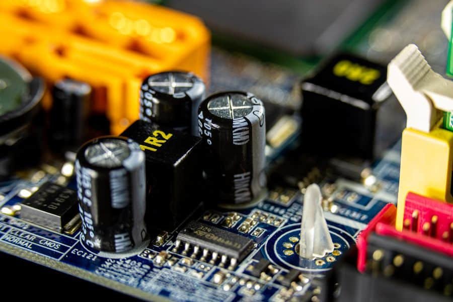
6. Optimize Component Placement for Reliability
Strategically place components to minimize stress and facilitate maintenance. Maintain 1-2mm clearance around sensitive components (e.g., BGAs, QFNs) to allow for rework and prevent solder joint cracks in high-vibration environments, per IPC-A-610. Avoid placing heavy components near board edges, where flexing can cause failures. For example, a poorly placed power IC near a board corner led to a 12% failure rate in a telecom PCB due to mechanical stress.
7. Ensure Uniform Component Orientation
Align components in the same direction and polarity to streamline automated assembly. For passive components like resistors, orient the long axis perpendicular to the PCB’s travel direction during soldering to prevent tombstoning (where one end lifts). For ICs like SOICs, align pin 1 markings parallel to the board’s travel direction, per IPC-7351. Uniform orientation reduces placement errors by up to 25% and speeds up assembly.
8. Prioritize Thermal Management in Layout
Place power-hungry components (e.g., power MOSFETs, voltage regulators) near board edges or ventilation areas to dissipate heat. Use thermal vias (0.3mm diameter, 1mm pitch) under high-power components to transfer heat to a ground plane, per IPC-2222. Simulate thermal performance using tools like Ansys or Altium’s PDN Analyzer to avoid hot spots. In a real-world case, poor thermal placement caused a 15°C temperature rise, leading to premature component failure in an industrial PCB.
9. Specify Robust PCB Physical Characteristics
Design PCB physical attributes to ensure stability and manufacturability:
- Outline and Thickness: Use standard sizes (e.g., 250mm width for wave soldering, 330mm x 250mm for reflow) and a thickness of 1.6mm or 2.0mm for larger boards to prevent deformation, per IPC-2221. Chamfer corners with a 3-5mm radius for safety.
- Warpage Control: Limit warpage to 0.75% (0.0075mm/mm) to ensure accurate component placement, per IPC-TM-650. Excessive warpage can disrupt SMT assembly.
- Positioning Holes: Include 2-4 non-metallized holes (2.5mm diameter) with 1mm clearance from traces to secure boards during assembly.
This ensures compatibility with manufacturing equipment and minimizes defects.
10. Streamline Panelization and Trace Design
Optimize panelization and trace design for efficient production:
- Panelization: Use V-grooves or tab-routing for easy board separation, keeping critical traces 2mm from separation lines to avoid damage, per IPC-2222. Include 3-5mm clamping edges for automated handling.
- Trace Design: Set minimum trace widths (e.g., 0.15mm for 1oz copper) to prevent corrosion and ensure signal integrity, per IPC-2221. Use differential pair routing for high-speed signals to maintain impedance control.
In a case study, poor panelization design caused trace damage during depaneling, increasing scrap rates by 10%. Proper panelization and trace design streamline production and reduce waste.
Advanced DFM Considerations
To further enhance manufacturability, consider Design for Test (DFT) and material selection:
- Design for Test (DFT): Add test points (1mm diameter, 2mm spacing) for in-circuit testing (ICT) to verify functionality, per IPC-9252. This reduces debugging time post-assembly.
- Material Selection: Choose FR-4 for standard applications or high-Tg materials (e.g., IT-180A, Tg 170°C) for high-temperature environments to prevent delamination. Ensure materials comply with RoHS and UL standards.
- HDI PCBs: For high-density designs, use microvias (0.1mm diameter) and buried vias to increase routing density, but verify manufacturer capabilities, as HDI requires advanced equipment.
These considerations address emerging trends like miniaturization and high-speed electronics, ensuring your design remains future-proof.
Conclusion
Optimizing PCB design for manufacturability requires careful attention to component selection, assembly methods, layout, and physical specifications. By applying these 10 DFM tips, designers can reduce costs, minimize defects, and accelerate production. From standardizing components to streamlining panelization, each tip contributes to high-quality, scalable PCBs. For expert PCB manufacturing that leverages DFM principles, contact JHYPCB for a free DFM consultation or quote. Let us help you bring your designs to life with precision and efficiency.
Advanced Learning:
- Basic Knowledge of PCB Pad Design
- PCB Terminology Glossary
- PCB Design Software Free Download
- What are the aspects of PCB Design For Manufacturing (DFM) and Design For Assembly (DFA)?
- Design For Manufacturability And Assemblability Of Printed Circuit Board
- A Free Software for PCB Design for Manufacturing or DFM Analysis
- Finding the Right China PCB Manufacturers:5 Vetting Tips
- Guide to Multilayer PCB Layer Stackup and thickness
- What does PCB open Circuit Mean?


