


Table of Contents
Introduction to PCB Open Circuits
Have you ever faced costly delays or customer complaints due to PCB defects? In the fast-paced world of electronics manufacturing, a PCB open circuit is one of the most common yet frustrating issues that can disrupt production and quality. A PCB open circuit occurs when two points on a circuit board that should be electrically connected—such as point A and point B—are not, breaking the flow of current and causing device malfunctions. This defect leads to insufficient shipments, rework, delivery delays, and even scrapped boards, posing significant challenges for manufacturers.
Understanding PCB open circuits, their causes, and prevention strategies is critical for anyone involved in PCB design, production, or quality control. In this guide, we’ll explore the types of open circuits, their root causes, and practical solutions to minimize their impact. Whether you’re a PCB manufacturer or an electronics enthusiast, you’ll find expert insights to improve your processes and ensure high-quality circuit boards.
What is a PCB Open Circuit?
A PCB open circuit is a critical defect in printed circuit board manufacturing where an intended electrical connection between two points—such as point A and point B—fails to form, interrupting the flow of current. This break in the conductive path can cause devices to malfunction, fail testing, or become entirely non-functional. In essence, an open circuit is the opposite of a short circuit, where unintended connections occur.
Open circuits typically manifest as gaps, breaks, or incomplete traces in the PCB’s copper pathways. Common symptoms include non-working components, inconsistent performance, or complete device failure. For manufacturers, the consequences are severe: scrapped boards, production delays, and increased costs due to rework or customer returns. These defects often stem from issues in the exposure, etching, or handling processes during PCB fabrication.
Understanding the nature of PCB open circuits is the first step toward effective detection and prevention. By identifying their symptoms and impacts, manufacturers can implement robust quality control measures to ensure reliable circuit boards.
Types of PCB Open Circuits
PCB open circuits manifest in various forms, each with distinct characteristics, causes, and solutions. Understanding these types is essential for diagnosing and preventing defects in PCB manufacturing. Below are the four primary types of PCB open circuits, along with their causes and recommended fixes.
1. Repeated Open Circuit
This type occurs when the same open circuit appears at the identical location on nearly every PCB in a batch, often with the same exposure film number. The root cause is typically a defect in the exposure film, such as a scratch or contamination, which transfers the flaw to each board during production.
- Solution: Scrap the defective exposure film and replace it with a new one. Strengthen Automated Optical Inspection (AOI) checks for the first and last boards in each batch to confirm the initial PCB is defect-free before full-scale exposure.
- Impact: Consistent defects lead to high scrap rates and production delays if not caught early.
2. Gap Open Circuit
A gap open circuit is characterized by a visible break or gap in a copper trace, reducing the line width to half or less of the standard width. Like repeated open circuits, this issue often stems from defects in the exposure film, such as dust or improper alignment.
- Solution: Replace the faulty exposure film and enhance AOI detection during the exposure process to identify gaps early. Regular film maintenance can prevent recurrence.
- Impact: Gaps compromise circuit reliability, often requiring board rework or scrapping.
3. Vacuum Open Circuit
In vacuum open circuits, multiple wires appear tapered or excessively thin, with some breaking entirely. This occurs when the exposure film and dry film are not in close contact with the PCB due to trapped air, caused by improper vacuum settings in the exposure table. Wires narrower than the customer’s minimum line width requirement result in scrapped boards.
- Solution: Ensure proper vacuum calibration before exposure and regularly inspect equipment to maintain airtight conditions. Operator training on vacuum systems is also critical.
- Impact: Tapering wires reduce board reliability and increase rejection rates during testing.
4. Scratched Open Circuit
Scratched open circuits are caused by physical damage to copper traces, often visible as scrape marks from external forces. Common causes include improper handling during production (e.g., incorrect board gripping) or malfunctioning machinery that scratches the PCB surface.
- Solution: Train operators on proper PCB handling techniques and implement regular maintenance for production equipment. Use protective covers during transport to minimize scratches.
- Impact: Scratches lead to immediate board failure and require costly rework or replacement.
By identifying the specific type of PCB open circuit, manufacturers can target their root causes and implement effective solutions, improving production quality and reducing waste.
Causes of PCB Open Circuits
Understanding the root causes of PCB open circuits is crucial for manufacturers aiming to improve quality and reduce defects in PCB production. These issues arise from a combination of material, process, human, and equipment-related factors. Below, we explore the primary causes contributing to open circuits, enabling targeted prevention strategies.
Material-Related Issues
Substandard materials are a leading cause of PCB open circuits. Poor-quality copper-clad laminates may have uneven surfaces or impurities, leading to incomplete etching or weak traces. Similarly, defective dry films or exposure films, such as those with scratches or contamination, can transfer flaws to the PCB during the exposure process, resulting in gaps or breaks.
Example: Dust on an exposure film can block UV light, causing incomplete trace formation.
Process-Related Issues
Errors during key manufacturing processes—exposure, development, and etching—frequently cause open circuits. For instance, improper exposure settings (e.g., incorrect UV intensity) can lead to underdeveloped traces, while over-etching may erode copper paths, creating gaps. Inconsistent development processes can also leave residual photoresist, disrupting circuit continuity.
Example: Over-etching can reduce line width below the required threshold, causing a gap open circuit.
Human Factors
Operator errors, such as improper handling or inadequate training, contribute significantly to open circuits. Mishandling PCBs during production (e.g., gripping boards incorrectly) can scratch copper traces, leading to scratched open circuits. Lack of adherence to standard operating procedures may also result in process deviations, exacerbating defects.
Example: An operator stacking boards carelessly can cause surface scratches, breaking critical traces.
Equipment Issues
Malfunctioning or poorly maintained equipment is another key culprit. Exposure tables with faulty vacuum systems can trap air between the film and PCB, causing vacuum open circuits with tapered or broken traces. Similarly, worn-out etching machines may produce uneven results, leading to incomplete circuits.
Example: A miscalibrated vacuum pump can result in air pockets, disrupting trace formation during exposure.
Addressing these causes requires a holistic approach, including high-quality materials, optimized processes, thorough operator training, and regular equipment maintenance. By tackling these issues, manufacturers can significantly reduce PCB open circuit occurrences and enhance production reliability.
How to Detect PCB Open Circuits
Detecting PCB open circuits early in the manufacturing process is critical to minimizing scrap, reducing costs, and ensuring high-quality PCBs. Various testing and inspection methods can identify these defects, from automated systems to manual checks. Below, we outline the most effective techniques for spotting open circuits, helping manufacturers maintain reliable production.
Automated Optical Inspection (AOI)
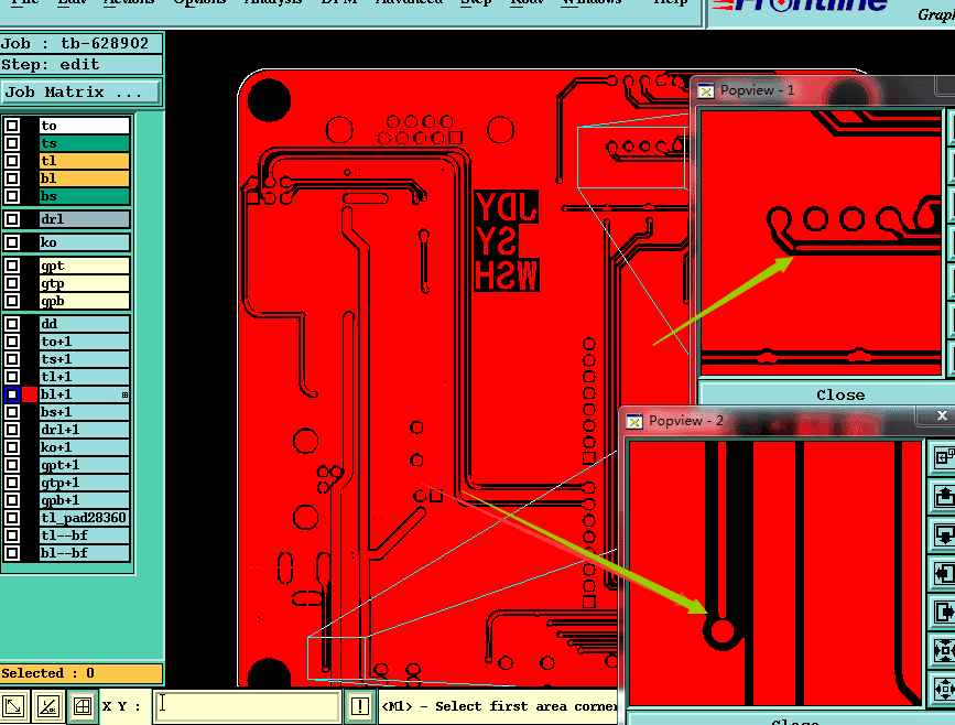
Automated Optical Inspection (AOI) is a widely used method for detecting PCB open circuits during production. AOI systems use high-resolution cameras and advanced algorithms to scan PCB surfaces, comparing them to a reference design. They can identify gaps, breaks, or thinned traces indicative of open circuits with high accuracy.
- Advantage: Fast and non-destructive, ideal for high-volume production.
- Application: Best for detecting repeated or gap open circuits during exposure or etching.
Flying Probe Testing
Flying probe testing is a versatile method for identifying open circuits, especially in prototypes or low-volume batches. This technique uses movable probes to test electrical continuity between points on the PCB, pinpointing breaks in the circuit path.
- Advantage: No need for custom fixtures, making it cost-effective for small runs.
- Application: Effective for detecting all types of open circuits, including scratched or vacuum defects.
X-Ray Inspection
X-ray inspection is essential for detecting hidden open circuits in multilayer PCBs, where internal layers are not visible. X-ray systems produce detailed images of the PCB’s internal structure, revealing breaks or incomplete traces in buried copper layers.
- Advantage: Non-destructive and highly precise for complex boards.
- Application: Ideal for identifying vacuum open circuits in multilayer designs.
Manual Visual Inspection
Manual visual inspection involves trained technicians examining PCBs under magnification to identify obvious open circuits, such as scratched traces or visible gaps. While less efficient than automated methods, it remains useful for small batches or as a secondary check.
- Advantage: Low-cost and accessible for initial defect screening.
- Application: Best for detecting scratched open circuits or large gaps.
By combining these detection methods, manufacturers can effectively identify PCB open circuits at various production stages, ensuring defects are caught before they impact final product quality.
How to Prevent PCB Open Circuits
Preventing PCB open circuits is essential for ensuring high-quality PCBs and minimizing production losses. By addressing the root causes—material defects, process errors, human factors, and equipment issues—manufacturers can significantly reduce the occurrence of open circuits. Below are proven strategies to prevent these defects and enhance PCB reliability.
Use High-Quality Materials
Selecting reliable materials is the first step in preventing open circuits. Opt for high-grade copper-clad laminates with consistent thickness and purity to ensure uniform etching. Use defect-free dry films and exposure films, regularly inspecting them for scratches, dust, or contamination that could cause repeated or gap open circuits.
Tip: Partner with trusted suppliers and verify material quality through incoming inspections.
Optimize Manufacturing Processes
Precise control over exposure, development, and etching processes is critical. Calibrate UV exposure settings to avoid underdeveloped traces, and monitor etching times to prevent over-etching, which can create gaps. Implement strict quality checks, such as AOI, at key stages to catch defects early.
Tip: Follow IPC standards (e.g., IPC-A-600) for process consistency and quality.
Enhance Operator Training
Human error, such as improper PCB handling, often leads to scratched open circuits. Train operators on correct handling techniques, such as using gloves and proper gripping methods, to avoid damaging copper traces. Regular training on standard operating procedures ensures adherence to best practices.
Tip: Conduct refresher courses and audits to maintain high operational standards.
Maintain and Calibrate Equipment
Faulty equipment, like exposure tables with poor vacuum systems, can cause vacuum open circuits. Perform regular maintenance on machinery, including vacuum pumps and etching systems, to ensure optimal performance. Calibrate equipment to maintain consistent settings and prevent process-related defects.
Tip: Schedule monthly equipment checks and keep detailed maintenance logs.
By implementing these strategies, manufacturers can proactively prevent PCB open circuits, improving yield rates and customer satisfaction. For more insights, download our free PCB defect prevention guide or contact our experts for tailored solutions.
FAQs About PCB Open Circuits
To address common queries about PCB open circuits, we’ve compiled answers to frequently asked questions. These insights help manufacturers, engineers, and enthusiasts better understand and manage this common PCB defect.
What is the most common cause of PCB open circuits?
The most common cause is defects in the exposure film, such as scratches or contamination, leading to repeated or gap open circuits. Other frequent causes include improper vacuum settings during exposure and physical damage from mishandling.
Can a PCB open circuit be repaired?
In some cases, yes. Scratched open circuits can sometimes be fixed by soldering a jumper wire to bridge the gap. However, repairs are often impractical for high-volume production or multilayer boards, making prevention critical.
How does AOI detect PCB open circuits?
Automated Optical Inspection (AOI) uses high-resolution cameras to compare PCB traces against a reference design. It identifies gaps, breaks, or thinned traces, making it effective for detecting repeated, gap, and vacuum open circuits during production.
What are the costs of PCB open circuit defects?
Open circuits lead to scrapped boards, rework, delayed shipments, and potential customer dissatisfaction. Costs vary depending on production volume, but defects can significantly impact profitability and reputation.
These FAQs provide a foundation for understanding PCB open circuit challenges. For deeper insights, explore our related resources or contact our team.
Conclusion
PCB open circuits are a persistent challenge in PCB manufacturing, causing delays, increased costs, and quality issues. By understanding their types—repeated, gap, vacuum, and scratched—and their causes, such as material defects, process errors, human factors, and equipment issues, manufacturers can take proactive steps to prevent them. Effective detection methods like AOI, flying probe testing, and X-ray inspection, combined with prevention strategies like using high-quality materials and rigorous training, ensure reliable circuit boards.
Investing in quality control and process optimization is key to minimizing PCB open circuit defects and enhancing production efficiency. For more expert tips, explore our resources on PCB testing and design, or contact us for tailored manufacturing solutions. Take the next step to improve your PCB quality today!


