


Standard PCB Thickness—All You Need to Know
- What is the Standard PCB Thickness?
- What are the factors that affect PCB thickness?
- What are the manufacturing factors that affect PCB thickness?
- Factors that Need to be Considered When Designing Non-standard Thickness PCBs
The standard thickness of the PCB board is about 1.57 mm or 0.062 inches, and it is usually referred to as 1.6mm. Although this is the most common thickness of the PCB, there may be thinner or thicker boards. There is a wide range of demanded thicknesses these days. It involves 0.031 inches, approximately 0.78 mm, and 0.093 inches, approximately 2.36 mm. The thickness of the PCB depends on the assembly requirements and the client’s choice for PCB fabrication.
The thickness of PCB influences the durability and performance of the board. PCBs with a certain standard or custom thickness must pass different tests of performance, reliability, durability, weight, and all in all quality. To be able to customize the thickness, you first need to gather your requirements and then decide if your PCB needs additional thickness or not.
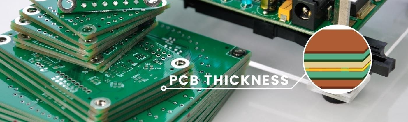
It is important to know about the standard thickness of the PCB board and why there is a need for a custom board. Your board may have a non-standard thickness due to design and manufacturing factors. Let us see the factors that impact the PCB thickness.
1) Copper Thickness
Standard copper thickness is about 1.4 to 2.8 mils (1-2 oz). The copper thickness depends on the current that you need to pass through the PCB. It is adjusted according to the requirements of the board.
The thickness of copper also affects the costs. The thicker the board, the more expensive it is because of material needs and processing.
2) Substrate
Substrate and laminate are the foundation or base of the PCB. The substrate is a non-conductive dielectric material with a dielectric composite structure. It is usually chosen according to the dielectric constant.
The common substrate consists of epoxy resin and paper. It is sometimes augmented by ceramics to enhance the dielectric constant. It allows the manufacturers to meet property requirements like glass transition temperature—the point where heat causes the material to soften and deform. Some standard substrates include FR-1 thru FR-6, G-10 and G-11, IMS (Insulated Metal Substrate), and many more.
Recommended Reading
- PCB Material Types
- What Is FR-4 Material In PCB Fabrication?
- Why is FR4 Used to Make High Tg PCBs?
- What is the Tg value of PCB substrate?
- Why choose FR4 as the general material of PCB?
- Complete Introduction of Flexible Circuit Board Materials
3) The Number of Layers of PCB
It is very well known and obvious that the layers of PCB affect the thickness. 2-6 layers PCB may have the standard thickness, but eight or more layers of PCB may not fall under the standard thickness of PCB. If a PCB requires more layers, don’t try to use thinner layers to achieve standard PCB thickness because it might become impractical. Allow PCB to be thicker so it can perform its functions.
Sometimes it is not necessary to increase the layers of PCB, so to achieve the required thickness parameters, you can reduce the layers and still manage to achieve the thickness you desire.


4) Signal Type
PCB uses a variety of signal types that determine the material needed for the board, and this affects the thickness of the board. For example, if a PCB carries high power signals, then it needs to be thicker and have wide copper traces. So, it means that the need for high power traces will result in a thicker PCB.
5) Types of Through Holes
To be able to make a compact design PCB, the vias route must trace through the board rather than on its surfaces. There are different types of thought holes, through via, micro via, blind via, buried via, and via-in-pad. The density and type of through holes play a major part in determining the thickness of the board.
6) Operating Environment
The conductivity and resistance of the board depend on the PCB thickness and materials it is made of. A thin PCB may not be suitable for rough and rugged operations.
PCB with thick copper traces is less thermally stable with a high current. Moreover, connectors and components of PCB also relate to the thickness of the board because of specific material and performance requirements. Depending on all these factors, the fabricator can decide if PCB needs a standard thickness or custom thickness.
Manufacturing Factors that Affect PCB Thickness Include:
Certain manufacturing factors affect the PCB thickness. Besides the design factors, there are also manufacturing capabilities that play an important role in the final design of the PCB.

1) Process Capability of Drilling Equipment
Fabricators or designers of PCB often concentrate on the size of drill holes and spacing due to performance points of view. A drill hole usually adds a layer of complexity to the PCB board. Whenever the manufacturers are drilling any kind of holes in the PCB, they are limited by the thickness of the board. Besides this limitation, they also have a diameter and depth capabilities limitation that depends on the milling machine.
The depth of the hole and drill hole diameter is usually in a ratio. This aspect ratio serves as a limitation. The standard ratio is 7:1 for standard drilling. However, some PCB manufacturers may have a greater aspect ratio, but it should be discussed before designing the PCB, and obviously, it comes with an extra cost.
2) Copper Thickness
Copper thickness is one the most important parts of PCB manufacturing. Copper traces are usually made with etching—the plating and etching of copper depending on the thickness of the internal copper layer. Thick copper layers will not only affect the pricing but will also have an impact on the manufacturability and design of the PCB.
3) Number of Layers
Anyone with technical knowledge of PCB will know that when there are more layers on the PCB, it is difficult to maintain the standard thickness of the board. However, different manufacturers use thinner layers to conclude a standard thickness, but it is not practical and may cost extra. You must make sure to discuss the capabilities and functionalities of PCB with the fabricator before finalizing the design and layering of PCB.
Factors that Need to be Considered When Designing Non-standard Thickness PCBs:
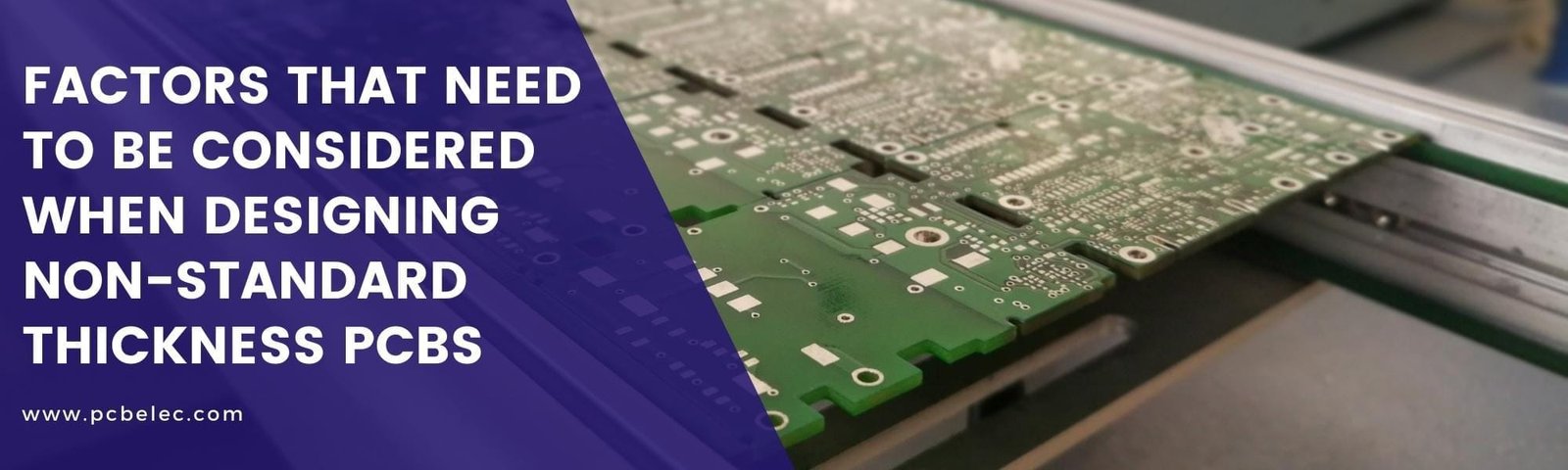
1) Process Capability of PCB Board Factory
One of the first things that you need is to check whether the manufacturer can create the thickness of the board that you need. Make sure they make certain thicknesses board to avoid any kind of problem in the stages ahead. It is better to research the manufacturer forehand and only entertain those who can create a PCB according to your requirements. However, any additional technique or requirement will cost you extra.
At JHYPCB, we can produce PCBs with a minimum board thickness of 0.3mm and a maximum of 3.0mm.
2) Additional Fees
First, you need to be sure that making a custom PCB will have an additional fee. Manufacturers charge more when you need a custom thickness. You need to assess the cost of the standard board and custom board and also their capabilities.
Order Any Type of PCB JHYPCB
JHYPCB is a one-stop solution for all PCB and assembly requirements. We can handle low-high volume orders and quick delivery. Our state-of-the-art facility is equipped with the latest machinery that is certified by ISO, UL, and RoHS. We have strict quality control to ensure the high-performance of the PCBs.
We can manufacture all types of PCBs and make assemblies. We offer fast prototypes and complete turnkey assembly services. Our aim is to deliver high-quality at a minimal cost. For more information, feel free to contact us.
Recommended Posts
16 Key Factors Affecting Flexible PCB Costs in 2025
Explore 16 factors affecting flexible PCB costs in 2025, including materials, layer count, and manufacturing processes. Learn cost-saving tips from JHYPCB experts.
Advantages of Multilayer PCB Design (and How Layer Count Impacts Cost from 2 to 10+ Layers)
Multilayer PCBs deliver better signal integrity, higher density, and more reliable power distribution than simple two‑layer boards—but they also affect cost. This article explains the real advantages of multilayer PCB design, when it makes sense to move from 2‑layer to 4/6/8+ layers, and how layer count influences manufacturing cost so you can choose the right stackup for your next project.
The Ultimate Guide to PCB Assembly in 2025: Process, Flow Chart, and Expert Insights
Dive into the 2025 PCB assembly process with our ultimate guide! Explore step-by-step insights, an interactive flow chart, and expert tips for SMT, HDI, and more. Learn how JHYPCB ensures quality for 5G and medical applications. Download our free DFM Checklist today!
4 Solutions to Reduce EMC in 6-layer PCB Design
In the EMC design of the PCB, the first important thing is the setting of the layers. The number of layers of the single board is composed of the number of power, ground, and signal layers.
Purple Circuit Board-Everything You Want To Know
The printed circuit board’s solder mask species the PCB’s color. Purple is one of many solder mask colors for printed circuit boards, which can have different colors depending on the application.
The Ultimate Guide to PCB Prototype Manufacturing: Everything You Need to Know
Looking for a reliable PCB prototype manufacturer? Look no further than JHYPCB. With years of experience and a commitment to quality, JHYPCB offers a comprehensive PCB prototype service that includes single-sided, double-sided, and multi-layered PCBs, as well as a variety of surface finishes and solder masks.