


Table of Contents
PCB vias are the unsung heroes of multilayer circuit boards, enabling seamless electrical connections across layers. From smartphones to automotive electronics, vias power the devices that drive our world. Whether you’re designing high-density PCBs for IoT or robust boards for aerospace, understanding via types—plated through holes, blind vias, and buried vias—is crucial for optimizing performance and cost. At JHYPCB, we specialize in delivering cutting-edge PCB fabrication solutions for global clients, ensuring precision and reliability in every project. Ready to elevate your PCB design? Explore the world of PCB vias and discover how JHYPCB can bring your ideas to life. Contact us for a free quote today!
What Are PCB Vias?
A PCB via is a small hole in a multilayer PCB that connects copper foil circuits across different layers, enabling electrical signals to flow seamlessly. In modern electronics, multilayer PCBs are essential for compact, high-performance devices like smartphones, medical equipment, and automotive systems. However, each copper layer is separated by an insulating material, making vias critical for creating reliable electrical connections between layers. Without vias, signals cannot travel efficiently, limiting the functionality of complex circuits.
Vias serve two primary purposes: facilitating electrical connections and, in some cases, securing components to the board. From enabling high-speed data transfer in 5G devices to powering intricate IoT modules, vias are the backbone of advanced PCB designs. At JHYPCB, we leverage state-of-the-art drilling and plating technologies to ensure precision in every via, meeting the diverse needs of global clients. Whether you’re a designer or manufacturer, understanding PCB vias is key to optimizing your next project.


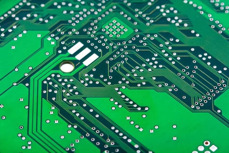
The printed circuit board is formed by stacking many layers of copper foil. These copper foil layers cannot communicate with each other because each layer of copper foil is covered with an insulating layer, so they need to rely on Vias for signal connection.


PCB Via Types
PCB vias are essential for connecting layers in multilayer printed circuit boards, and their types—plated through holes (PTH), blind vias, and buried vias—serve distinct roles in PCB fabrication. This section explores their definitions, manufacturing processes, applications, and trade-offs, helping designers and engineers choose the right via type for optimal performance, cost, and space efficiency. Understanding these PCB via types is key to mastering high-density interconnect (HDI) PCB design and meeting modern electronic demands.


Plated Through Hole (PTH)
A Plated Through Hole (PTH) is a via that spans the entire thickness of a PCB, connecting all layers with a copper-plated inner wall for robust electrical conductivity. Created through mechanical drilling or laser technology, PTHs are the simplest and most cost-effective via type, typically with minimum diameters of 0.15 mm (6 mil) for mechanical drilling. They are widely used for mounting through-hole components, such as connectors or resistors, and are ideal for traditional PCBs in consumer electronics, power supplies, and industrial controls. PTHs are easy to manufacture—drilling followed by electroplating—but occupy more space than other vias, limiting their use in compact, high-density designs. Their reliability and affordability make them a staple for applications where cost outweighs space constraints.

Blind Via Hole (BVH)
Blind Via Holes (BVHs) connect an outer layer of a PCB to one or more inner layers without penetrating the entire board. Formed using laser drilling for precision, blind vias maintain a controlled depth, often with a depth-to-diameter ratio of 1:1 to ensure uniform copper plating. With diameters as small as 0.1 mm (4 mil), they are critical for HDI PCB design, enabling compact layouts in devices like smartphones, tablets, and wearables. Blind vias save surface space by allowing additional routing or component placement, but their manufacturing is more complex and costly than PTHs due to precise drilling and alignment requirements. They excel in high-speed circuits where signal integrity is paramount, though careful design is needed to avoid plating issues.

Buried Via Hole
Buried Via Holes connect internal layers of a multilayer PCB without reaching the outer surfaces, remaining hidden within the board. These vias are formed before lamination by drilling and plating individual inner layers, then bonding them together, a process that demands advanced equipment and precise alignment. With diameters as small as 0.1 mm via laser drilling, buried vias are vital for HDI PCBs in complex applications like servers, aerospace electronics, and medical devices. They maximize surface space and reduce parasitic capacitance, enhancing signal integrity, but their intricate manufacturing increases costs. Buried vias are reserved for high-density designs where space efficiency and performance justify the added complexity.

Comparison and Considerations
Each via type offers unique advantages, as shown in the chart below. PTHs are cost-effective but space-intensive, while blind and buried vias enable compact HDI designs at higher costs. Designers must consider factors like layer count, signal speed, and budget when selecting via types. For instance, micro vias (a subset of blind/buried vias with diameters <0.15 mm) are increasingly popular in 5G and IoT applications for their precision.

PCB Via Design and Manufacturing
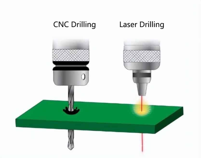
Designing and manufacturing PCB vias require precision to ensure electrical performance and reliability in multilayer printed circuit boards. Vias are created using mechanical or laser drilling, with the choice depending on the via type and board complexity. Mechanical drilling, suitable for plated through holes, achieves minimum diameters of 0.15 mm (6 mil) and is cost-effective for standard PCBs. Laser drilling, used for blind and buried vias in HDI PCBs, supports smaller diameters down to 0.1 mm (4 mil) but increases costs due to its precision. Via size is critical: smaller vias save space and reduce parasitic capacitance, ideal for high-speed circuits, but they demand advanced manufacturing techniques. Design rules, such as maintaining a depth-to-diameter ratio (e.g., 6:1 for mechanical drilling), ensure uniform copper plating and signal integrity. For high-current applications, larger vias (e.g., 0.5 mm) are preferred to handle thermal and electrical loads. Adhering to industry standards, like IPC guidelines, optimizes via performance while balancing cost and complexity in modern PCB designs.

Advantages of Blind and Buried Vias in Modern PCBs
Blind and buried vias, known as non-through vias, offer significant advantages in modern PCB design, particularly for HDI PCBs. By connecting specific layers without occupying the entire board thickness, these vias maximize surface space for components and routing, enabling compact designs critical for devices like smartphones, IoT modules, and medical equipment. Blind vias link outer layers to inner ones, while buried vias connect internal layers, reducing signal interference and improving electromagnetic compatibility (EMI) performance. Their smaller diameters, often as low as 0.1 mm via laser drilling, minimize parasitic capacitance, enhancing signal integrity for high-speed circuits. Additionally, non-through vias reduce the number of layers needed, lowering manufacturing costs in complex designs. These benefits make blind and buried vias essential for advanced applications, such as 5G infrastructure and automotive electronics, where space efficiency and performance are paramount.
FAQ on PCB Vias
What are PCB vias and their function?
PCB vias are holes in multilayer PCBs that connect copper layers, enabling electrical signal transmission. They ensure reliable interlayer communication, critical for devices like smartphones and automotive electronics.
What are the main types of PCB vias?
PCB vias include plated through holes (PTH), blind vias, and buried vias. PTHs connect all layers, blind vias link outer to inner layers, and buried vias connect internal layers for high-density designs.
What size are PCB vias?
Via sizes vary: plated through holes typically start at 0.15 mm (6 mil) for mechanical drilling, while blind and buried vias can be as small as 0.1 mm (4 mil) using laser drilling, depending on design needs.
What are the different types of micro vias?
Micro vias, used in HDI PCBs, include blind and buried vias with diameters below 0.15 mm. They are often laser-drilled for precision in compact devices like wearables and 5G modules.
What is the difference between stacked and staggered vias?
Stacked vias align vertically across multiple layers, ideal for compact HDI designs but complex to manufacture. Staggered vias are offset, simpler to produce but less space-efficient.
What are PCB filled and plugged vias?
Filled vias are packed with conductive or non-conductive material to enhance strength or thermal conductivity. Plugged vias are partially filled to prevent solder flow, often used in via-in-pad designs.
Conclusion
PCB vias—plated through holes, blind, and buried—are critical for enabling efficient electrical connections in multilayer PCBs, driving innovation in compact, high-performance electronics. From cost-effective PTHs to space-saving blind and buried vias, choosing the right via type optimizes design efficiency and signal integrity for applications like 5G devices and automotive systems. Understanding via design and manufacturing ensures better performance and cost management in PCB fabrication. Ready to enhance your PCB project? Explore professional PCB fabrication services or request a free design consultation today to bring your ideas to life!


