Table of Contents
Why DFM Matters Even More in Low Volume PCB Assembly
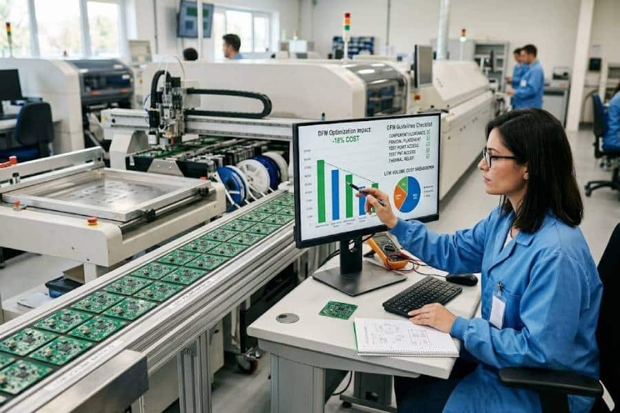
Design for Manufacturability (DFM) is one of the most powerful levers for controlling cost in low volume PCB assembly. When batches are small, setup time, engineering review, material choices, and assembly complexity all have a bigger impact on the price of each board. There are fewer units to absorb fixed costs, so any design decision that adds process steps or risk can quickly make a small build disproportionately expensive.
At the same time, low volume runs—whether for prototypes, pilot builds, or niche products—are often where designs are still changing. This makes DFM especially valuable: by simplifying stackup, matching manufacturer capabilities, optimizing panelization, and designing for efficient assembly and test, engineers can keep small-batch PCB builds cost-effective without compromising quality or reliability.
This article walks through practical DFM guidelines tailored specifically for low volume PCB assembly. It explains the unique cost drivers in small runs and provides concrete design rules you can apply to reduce cost, improve yields, and shorten time to market.
Understanding Cost Drivers in Low Volume PCB Assembly
Before diving into DFM guidelines, it helps to understand why low volume builds behave differently from large-scale production from a cost perspective.
Fixed vs Variable Costs in Small-Batch Builds
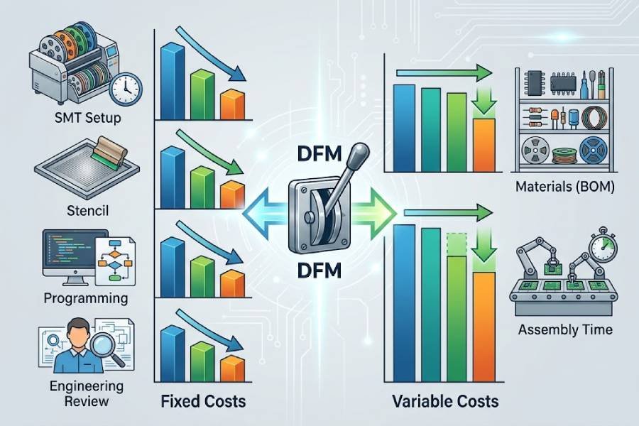
Every PCB assembly run includes fixed costs: SMT line setup, stencil preparation, pick-and-place programming, engineering review, and initial quality checks. In high-volume production, these costs are spread across thousands of boards and become negligible per unit. In low volume assembly, the same fixed activities may be amortized over just dozens or hundreds of units, causing the per-board cost to rise sharply.
DFM cannot eliminate fixed costs, but it can minimize the time and complexity associated with them. Designs that fit within a manufacturer’s standard capabilities, require fewer special steps, and share common tooling or programs across variants make it easier to keep low volume setups efficient and affordable.
Fabrication Complexity and Stackup Choices
On the fabrication side, design complexity is another major cost driver. Higher layer counts, exotic laminates, controlled-impedance stackups, heavy copper, tight mechanical tolerances, and special finishes all add cost. In large volumes, these premiums may be justified or partially offset by economies of scale. In low volume, every additional complexity tends to have a noticeable impact on the price of each panel.
Not every application can use a simple, standard board, but many can avoid over-specifying stackup and tolerances. Aligning design requirements with what the fabricator can achieve easily and repeatedly is central to DFM for cost-effective small batches.
Assembly Complexity, Components, and Manual Work
Assembly complexity is just as important. Double-sided SMT, mixed technologies (SMT plus dense through-hole), specialized connectors, large mechanical parts, and odd-form components usually require more handling, custom tooling, or manual operations. In low volume builds, the labor associated with these steps cannot be spread across many units, making each board more expensive.
DFM for assembly focuses on minimizing unnecessary complexity and ensuring that whatever complexity remains can be handled efficiently with available equipment. Choices around footprint, component placement, and BOM structure play a direct role in how much time the assembler must spend per board.
DFM Guidelines for PCB Fabrication in Low Volume Builds
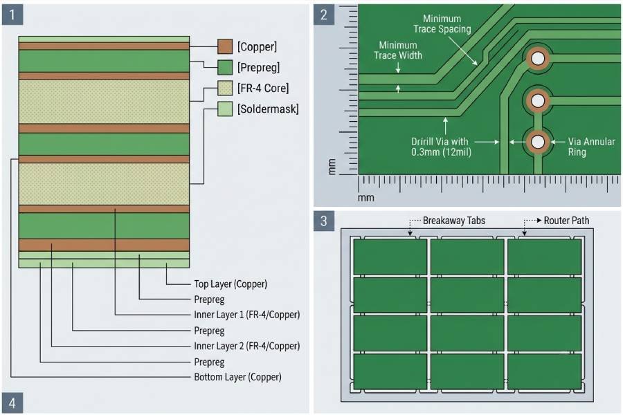
The first layer of DFM for cost-effective low volume assembly is at the PCB fabrication level. Optimizing stackup, design rules, and panelization can avoid stepping into higher-cost process categories and can improve yields, which is especially critical when there are fewer units to work with.
Simplify Layer Count and Stackup
Where performance allows, keep the PCB layer count as low as practical. Moving from a four-layer to a six-layer stackup, or from simple two-layer boards to more complex constructions, adds material and processing cost that become highly visible in small runs.
Whenever possible, use:
- Standard FR‑4 materials
- Common board thicknesses such as 1.6 mm
- Standard copper weights rather than heavy copper
These choices align with fabricators’ default process windows and avoid special handling, which reduces both cost and risk in low volumes.
Controlled impedance, special dielectrics, or rigid-flex structures are sometimes required. In those cases, involve the fabricator early to confirm which constructions are most cost-effective at the intended volumes.
Use Standard Design Rules Where Possible
DFM aims to keep critical features within standard capability ranges instead of pushing toward the process limits. For low volume cost control, this means avoiding unnecessarily tight rules on:
- Minimum trace width and spacing
- Minimum via drill size and pad size
- Annular ring and copper-to-edge clearances
Using a fabricator’s standard trace/space (for example 6/6 mil or 4/4 mil, depending on the shop) and commonly supported via sizes helps avoid moving into “advanced” process categories that carry higher pricing and potentially lower yields.
Likewise, blind and buried vias, microvias, and complex milling should only be used when they are truly required for density or performance. In many low volume designs, careful layer planning and placement can avoid these cost multipliers.
Optimize Board Size, Shape, and Panelization
Board outline and panelization strategy strongly influence low volume cost because they affect material usage and how efficiently panels can be processed. Simple, rectangular or near-rectangular outlines are usually the most economical. Irregular shapes, internal cutouts, and complex routing increase fabrication time and can reduce panel utilization.
DFM guidelines for cost-effective panelization include:
- Designing board dimensions that nest efficiently into the fabricator’s standard panel sizes
- Using straight edges and consistent margins to allow V-score or straightforward routing
- Minimizing internal slots and complex profiles unless functionally required
Especially for low volume, improving panel utilization by even a small margin can have a noticeable effect on per-board cost.
Keep Drill and Via Strategy Cost-Aware
Drilling is a relatively expensive process step, and in low volume every extra tool change or special hole type matters. To keep costs in check:
- Minimize the number of distinct drill sizes in the design
- Avoid extremely small holes that require special tooling or slower feeds
- Maintain adequate annular rings and spacing to support good yields
Where possible, standardize on a small set of via and plated-through hole sizes that the fabricator can produce reliably without stepping into higher-cost categories.
DFM Guidelines for PCB Assembly in Low Volume Builds
Assembly-focused DFM has a direct impact on how much time and effort is required to build each board. For low volume runs, where setup and handling dominate the cost structure, small improvements in assembly efficiency can significantly reduce per-unit pricing.
Optimize Component Selection for Availability and Cost
Component choice affects not only BOM cost but also assembly and sourcing complexity. In low volumes, sourcing small quantities of exotic or niche components can involve longer lead times, higher unit prices, and additional handling steps. DFM guidelines for component selection include:
- Favoring common, widely available packages such as 0603/0805 passives and standard IC footprints
- Minimizing the number of unique part numbers (NPIs) in the BOM to simplify procurement and kitting
- Avoiding unnecessary package diversity for functionally similar parts
Selecting components that are well supported by automated assembly and common stocking policies reduces both procurement overhead and the risk of delays or substitutions in low volume builds.
Reduce Assembly Complexity: Sides, Mixes, and Manual Operations
The more process steps and manual interventions required per board, the higher the cost, especially at small volumes. To keep assembly efficient:
- Place as many components as possible on a single side of the PCB to reduce the number of print-and-reflow cycles
- Group through-hole components logically to allow wave soldering or selective soldering where feasible, rather than relying heavily on hand soldering
- Avoid unnecessary odd-form or mechanical parts that require special fixtures or time-consuming manual handling
Double-sided SMT and extensive hand assembly may be unavoidable in some designs, but DFM seeks to minimize them and ensure that when they occur, they are handled in a structured, repeatable way.
Component Placement, Spacing, and Orientation for Yield
Good component placement practices support both assembly yield and inspection coverage. For low volume assemblies, where each extra rework or debug cycle is costly, these details matter:
- Maintain adequate spacing between components for pick-and-place, soldering, and rework tools
- Keep sufficient clearance from board edges, cutouts, and mechanical features
- Standardize component orientation where possible (for example, aligning polarized capacitors, LEDs, and IC pin 1 in consistent directions)
These practices reduce the chance of placement or orientation errors and make AOI programming more straightforward, which is particularly beneficial when only a small number of panels are run.
Design for Testability and Fewer Debug Cycles
In low volume assembly, each board that needs extensive debugging or rework has a disproportionate impact on total cost. Designing for testability helps catch issues quickly and reduces the time required to validate each build:
- Provide accessible test points for key nets such as power rails, critical signals, and communication buses
- Ensure test pads or connectors are positioned so that flying probe, ICT, or functional test fixtures can reach them
- Consider including simple onboard test features, such as LEDs or test headers, that help verify basic functionality quickly
A design that can be tested efficiently is easier to bring up during small-batch production and less likely to require repeated troubleshooting, which saves both time and money.

Panelization Strategies That Save Money in Low Volume PCB Assembly
Panelization is especially important in low volume because it determines how efficiently both fabrication and assembly steps can be applied to a limited number of boards.
Designing for Shared Panels and Multi-Design Options
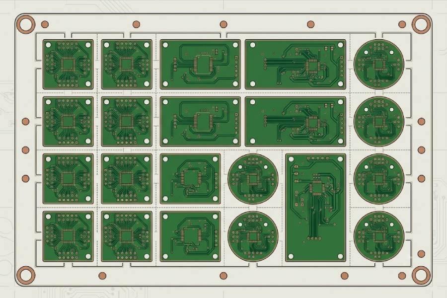
For small batches, it is often cost-effective to place multiple board images on a single panel. This can include:
- Multiple copies of the same board to reduce handling and line stops
- Different board variants or related designs arranged on one shared panel
When planned carefully, multi-design panels allow setup and tooling costs to be spread across several SKUs at once. This approach is particularly attractive for families of boards that share common dimensions or connector locations.
Balancing Handling, Yield, and Depaneling
Aggressively packing boards into a panel is not the only concern. DFM must also consider how panels will be handled and separated:
- Allow sufficient spacing between boards for routing tools or V-scoring
- Include tooling holes and fiducials for stable handling and accurate alignment
- Ensure that breakaway tabs, slots, and V-score lines do not create stress concentrations that can crack solder joints or damage components during depaneling
By designing panels that are both efficient and robust, engineers can avoid damage during separation and reduce rework, which is especially valuable when the number of boards is limited.
Collaborating With Your PCB Manufacturer on DFM for Low Volume
Even the best internal DFM practices benefit from close collaboration with the chosen PCB manufacturer. For low volume projects, where each iteration carries relatively high per-unit costs, early communication can prevent expensive surprises.
Share Design Files Early and Request DFM Review
Rather than waiting until a design is “finished” to involve the manufacturer, it is often more cost-effective to share preliminary Gerber data, stackup concepts, and assembly drawings for a DFM review. Many PCB suppliers provide DFM feedback as part of their service, particularly for small-batch and NPI projects.
By addressing potential issues—such as problematic clearances, marginal drill sizes, or assembly bottlenecks—before a low volume build starts, teams can avoid failed runs and re-spins that would otherwise consume limited budgets.
Align on Standard Capabilities and Cost Tiers
Each manufacturer has standard capability “tiers” for fabrication and assembly. Understanding these tiers helps designers stay within the most cost-effective process window. Key topics to clarify include:
- Standard and advanced trace/space and via sizes
- Supported board thicknesses and copper weights
- Default panel sizes and preferred panelization approaches
- Standard surface finishes (for example, HASL vs ENIG) and their cost implications
DFM guidelines should be tailored to these capabilities so that the final design does not inadvertently require special processing reserved for high-complexity or low-yield work.
Design Iterations Optimized for Small Batches
Low volume builds are often part of an iterative development cycle. From a DFM perspective, it is more efficient to:
- Consolidate design changes between runs instead of issuing many tiny revisions
- Prioritize changes that directly address manufacturability, yield, or major functional issues
- Use feedback from the assembler—such as defect trends or test results—to guide which modifications will have the biggest impact
For customers, this means treating each low volume build as a learning opportunity and capturing insights before committing to the next iteration.

Practical DFM Checklist for Cost-Effective Low Volume PCB Assembly
The following checklist summarizes key DFM guidelines discussed above. Applying these points during design can significantly improve the cost and success rate of low volume PCB assembly:
- Keep layer count as low as performance allows; avoid complex stackups unless truly required.
- Use standard FR‑4, common board thicknesses, and standard copper weights wherever possible.
- Stay within the manufacturer’s standard trace/space and via capabilities to avoid higher-cost process tiers.
- Minimize unique drill sizes and avoid blind/buried vias and microvias unless density or performance demands them.
- Design board outlines and dimensions for efficient panelization on the fabricator’s standard panel sizes.
- Favor simple, rectangular outlines and avoid unnecessary internal cutouts or complex shapes.
- Place as many components as possible on one side of the board to reduce assembly steps.
- Use common, widely available component packages and reduce the number of unique part numbers in the BOM.
- Maintain adequate component spacing and consistent orientation to support automated placement, soldering, and inspection.
- Provide accessible test points and consider how flying probe, ICT, or functional testing will access key nets.
- Share design data early with your manufacturer and request a DFM review before committing to a low volume run.
- Align design rules with the manufacturer’s standard capabilities and cost structure to avoid unintentional complexity.
Conclusion
Low volume PCB assembly does not have to be inherently expensive or risky. By applying thoughtful DFM guidelines that account for the unique cost structure of small-batch builds, engineers can simplify fabrication, streamline assembly, and reduce debug and rework—without sacrificing quality or reliability.
From stackup and design rules to component selection, panelization, and testability, each decision made during the design phase influences how efficiently a low volume build can be executed. When these decisions are aligned with the manufacturer’s capabilities and backed by collaborative DFM review, low volume PCB assembly becomes a practical, cost-effective way to validate designs, support niche products, and bridge the gap between prototype and larger-scale production.