Table of Contents
What Is Low Cost PCB Assembly?
Low cost PCB assembly refers to a cost‑conscious way of building and populating printed circuit boards, where design decisions, sourcing choices, and process planning are all used to reduce total assembly cost—without simply cutting corners on workmanship or inspection.
In practice, it means looking at the entire project—from PCB layout and BOM preparation to assembly methods and testing—and asking where cost can be optimized while still meeting the reliability and performance requirements of the end product.
For many engineering teams and buyers, low cost PCB assembly is most relevant in prototype, low‑volume, and cost‑sensitive turnkey projects, where budgets are tight but boards still need to function correctly and be built with stable processes.
In these contexts, the “low cost” label is less about the absolute cheapest quote and more about using manufacturing know‑how and DFM/DFMA thinking to avoid unnecessary expense—extra layers, excessive through‑hole parts, overly complex panelization, or over‑specified testing that does not match project risk.
When low cost PCB assembly is approached as a structured method rather than a price race, it becomes a practical way to free budget for more iterations, additional prototypes, or parallel projects, while keeping essential quality expectations intact.
Key Factors That Drive PCB Assembly Cost
Even without changing fabricator or assembler, PCB assembly cost is strongly influenced by a few core factors: board design and layout, component selection, assembly processes, and the level of testing and inspection required.
Understanding how each factor contributes to cost makes it much easier to apply low‑cost strategies that genuinely reduce spend instead of shifting expenses to other parts of the project.
Board Design and Layout
The way a PCB is designed and laid out has a direct impact on assembly cost. Board size, shape, layer count, routing density, and whether SMT components are on one or both sides all affect how many assembly steps are needed and how complex those steps become.
For example, placing SMT components on a single side and avoiding unnecessary board irregular shapes can reduce reflow cycles, panel handling complexity, and fixture requirements, which translates into lower process and labor costs.
Component Types and Package Sizes
The types of components used and their package sizes also play a major role. Very small passives, fine‑pitch ICs, BGA packages, and large numbers of through‑hole parts require more precise placement, more careful soldering, and often more intensive inspection.
Using standard package sizes where practical, limiting very fine‑pitch parts to where they are truly needed, and reducing unnecessary through‑hole usage can make assembly more automated and repeatable, which tends to lower per‑board costs.
Assembly Processes and Steps
PCB assembly cost is closely tied to which assembly processes are required and how many times a board must pass through them.
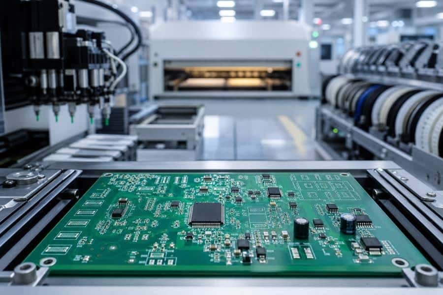
Automated SMT reflow is usually the most cost‑effective for large numbers of similar boards, while wave soldering, selective soldering, and manual soldering add complexity and labor—especially when boards mix dense SMT areas with scattered through‑hole connectors and mechanical parts.
Each additional assembly step (second‑side reflow, extra selective soldering passes, hand rework) adds time and cost, so process simplification is a core part of any low cost PCB assembly method.
Testing and Inspection Level
Finally, the testing and inspection strategy for a project has a significant cost impact. Automated optical inspection (AOI), X‑ray inspection, in‑circuit testing (ICT), and functional testing all provide different levels of coverage at different price points.
For some cost‑sensitive prototypes, AOI combined with visual checks may be sufficient, whereas safety‑critical or high‑reliability boards may justify ICT, FCT, and X‑ray despite the added expense.
Choosing inspection and test levels that match the actual risk profile of the project, rather than applying the same deep test regime to every board, is an important lever in achieving low cost PCB assembly without undermining reliability.
Design and Layout Methods for Low Cost PCB Assembly
Once you understand what drives assembly cost, the most direct way to achieve low cost PCB assembly is to start at the design stage: layout decisions, panelization, and how components are distributed across the board often have more impact on cost than the choice of assembler itself.
Design for manufacturability and assembly (DFM/DFA) is essentially about removing avoidable complexity—extra layers, awkward shapes, difficult placements—so that standard processes and tooling can do more of the work at lower cost.
Place SMT Components on a Single Side Where Practical
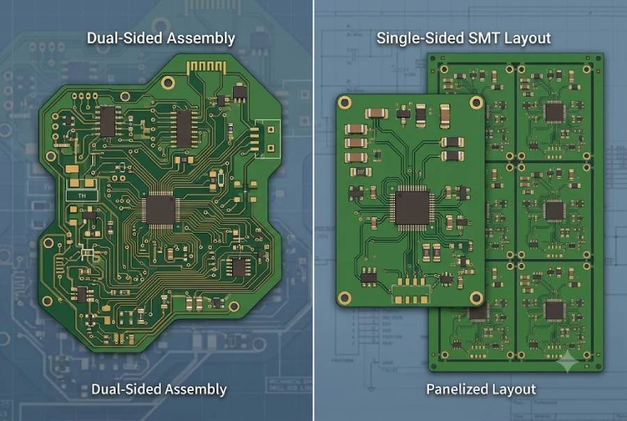
Putting most SMT components on a single side of the PCB, instead of spreading them across both sides, simplifies the assembly flow and can significantly lower cost.
Single‑sided SMT layout typically means one reflow pass instead of two, fewer fixture changes, and less opportunity for solder defects during later handling or testing, all of which reduce process time and rework risk.
For prototype and low‑volume builds, where budgets are tight and yield learning is important, keeping SMT on one side whenever the electrical and mechanical design allow is one of the most straightforward low‑cost layout decisions you can make.
Use Standard Package Sizes and Unified Orientation
The choice of package sizes and how they are oriented on the board heavily influences assembly difficulty. Very small passives (such as 0402) and fine‑pitch ICs are harder to place and inspect than more standard packages like 0603 or 0805, and they often require tighter process windows to avoid defects.
Industry cost‑reduction guides consistently show that switching from ultra‑small passives to more standard sizes, and avoiding unnecessarily fine‑pitch or lead‑less packages unless they are truly needed, can easily trim assembly cost by 10–15% without changing circuit behaviour.
At the same time, keeping component orientation as unified as possible—for example, aligning polarized parts and consistent pin‑1 direction in a region—helps automated equipment place parts faster and makes visual inspection more reliable.
From a low‑cost perspective, standardizing package families and orientations reduces programming and inspection complexity, which is especially valuable in mixed SMT/THT designs or small production runs.
Panelize the PCB for Efficient Assembly
Panelization—combining multiple boards into a single panel for fabrication and assembly—is a classic technique for reducing per‑board cost.
By designing PCBs to fit efficiently onto a standard panel size, you improve material utilization, reduce handling time, and allow pick‑and‑place and soldering operations to work on several boards at once rather than one at a time.
Good panelization practice includes using consistent board sizes and shapes where possible, choosing an appropriate panel size for the expected build volume, and selecting a cost‑effective depanelization method (such as V‑groove scoring for rectangular boards or tab‑routing for irregular shapes).
From a low‑cost assembly viewpoint, collaborating with your manufacturing partner on panel layout early—before finalising outline and mounting features—often yields some of the easiest and most impactful cost savings.
Optimize Board Size and Shape
Board dimensions and outline shape may seem like fabrication concerns, but they also directly affect assembly cost: larger boards require more panel area, more travel time under machines, and often more fixture complexity.
Designing PCBs to be as compact as practical, within the constraints of signal integrity, creepage/clearance, and mechanical requirements, can reduce material use and shorten assembly time, especially in multi‑panel production.
Where possible, avoiding highly irregular outlines or complex cut‑outs also helps. Standard rectangular or tessellating shapes generally panelize better and can use simpler depanelization techniques, which means less waste and lower per‑board assembly cost.
In cost‑sensitive projects, it often makes sense to treat board size and shape as part of the DFM negotiation—adjusting mechanical features slightly to unlock easier panelization and faster assembly.
Limit Unnecessary Through‑Hole Usage
Through‑hole technology (THT) still has an important role for connectors, high‑current parts, and certain mechanical interfaces, but large numbers of THT components are inherently more labour‑intensive to assemble than equivalent SMT parts.
Each additional wave soldering, selective soldering, or manual soldering step extends process time and adds potential rework, so low cost PCB assembly strategies typically aim to reserve THT for where it adds clear technical value and move purely functional, low‑stress parts to SMT when feasible.
Reducing unnecessary THT usage can allow more of the assembly to be handled in automated SMT lines, which are usually more efficient and consistent per unit cost, especially for small and mid‑volume runs.
In practice, this often means re‑evaluating legacy designs and asking whether certain resistors, capacitors, and non‑critical components can migrate from through‑hole to SMT packages without affecting performance.
BOM and Component Sourcing Strategies for Low Cost PCB Assembly
In most real projects, the bill of materials (BOM) and component sourcing strategy account for the largest share of PCB assembly cost, often 60–70% of total expenses.
That means low cost PCB assembly is not only about layout and process choices; it also depends heavily on how clean, structured, and sourcing‑friendly your BOM is, and whether you use turnkey or consigned models in a way that fits your team and project.
Provide a Complete and Well‑Structured BOM
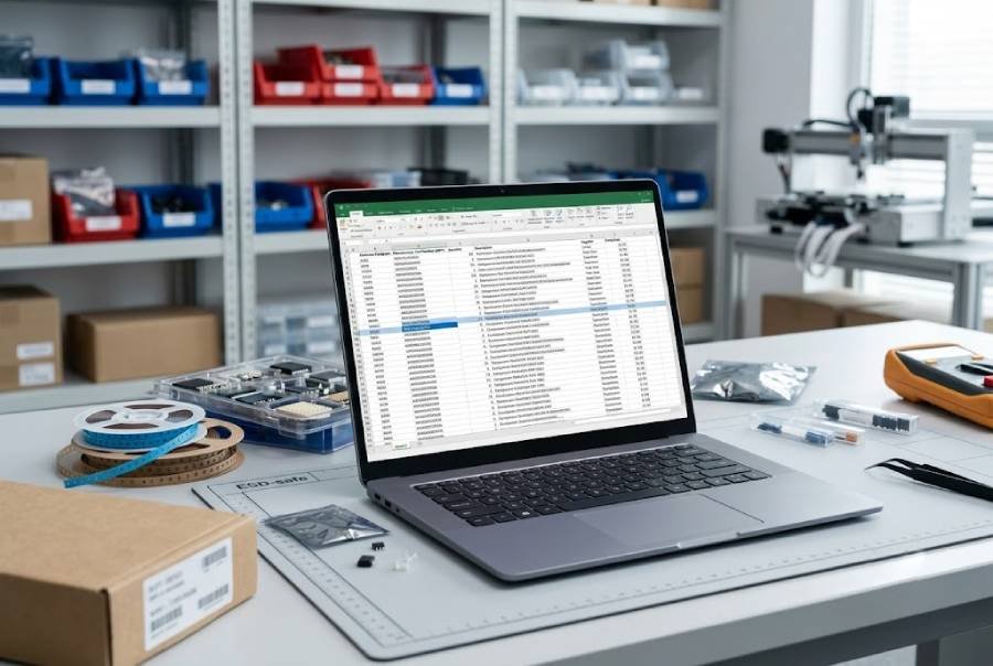
A complete, well‑structured BOM is one of the strongest levers for both fast quoting and cost‑effective assembly.
Industry guidance repeatedly emphasizes that a good PCB assembly BOM should include at least: line item number, quantity per assembly, reference designators, manufacturer part number, description, package/footprint, and any notes on alternates or “do not populate” (DNP) parts.
When BOMs are incomplete—missing part numbers, ambiguous descriptions, or lacking package information—assemblers must spend more time clarifying data, checking compatibility, and sometimes re‑quoting, which increases overhead and can delay production.
From a low‑cost perspective, grouping identical parts on a single BOM line, listing all reference designators clearly, and validating MPNs before handoff are simple steps that improve procurement efficiency and reduce the risk of mis‑assembly or last‑minute changes.
Simplify the BOM Where It Makes Sense
Beyond structure, BOM simplification is a proven method to lower assembly cost without compromising function.
Standardizing on a core set of components across multiple designs, avoiding overspecified parts (such as precision components where general‑purpose ones are sufficient), and reducing the number of unique part numbers all help consolidate orders and improve pricing.
Guides on PCB assembly cost reduction often recommend avoiding obsolete or end‑of‑life parts, preferring widely available, multi‑sourced components, and aligning tolerances and ratings with actual design needs rather than worst‑case over‑specification.
For low cost PCB assembly, this kind of BOM simplification makes sourcing more resilient, reduces the chance of surprises during procurement, and allows assemblers to leverage better pricing across larger, more consistent component volumes.
Use Turnkey and Consigned Models Strategically
How components are sourced—by the assembler (turnkey) or by the customer (consigned)—also influences cost and risk.
In a full turnkey model, the assembler’s purchasing team quotes the BOM across its distributor network, manages logistics, and applies a procurement markup to cover sourcing workload; this can simplify projects and avoid hidden costs from fragmented purchasing.
Consigned or partial turnkey models give design teams more direct control over component choices and supplier relationships, but they also shift kitting effort, inventory management, and supply risk back to the customer side.
From a low‑cost perspective, many small teams find that using turnkey for standard parts and consigned for critical or specialty components provides a good balance: the assembler can optimize pricing on common items, while the customer retains control over sensitive or strategic parts.
Collaborate on Approved Alternates and Sourcing Flexibility
Finally, smart sourcing strategies for low cost PCB assembly almost always involve approved alternates and multi‑source planning.
By including vetted alternates in the BOM—parts that share the same footprint and key specifications—you give assemblers flexibility to switch between components when supply or pricing changes, without requiring board redesign.
Industry recommendations consistently highlight that aligning BOM choices with readily available, competitively priced components, and working with authorized distributors for traceability and quality, are key to keeping assembly costs down while protecting schedule and reliability.
In practice, early collaboration with your assembly partner on potential substitutions and supply chain risks allows them to flag problematic parts before build, suggest alternatives, and help you maintain both cost targets and delivery dates.
Process and Inspection Choices for Cost-Sensitive Projects
For cost‑sensitive PCB assemblies, which processes you run and how far you go with inspection and testing can dramatically change total project cost.
Low cost PCB assembly is not about removing inspection or using the cheapest possible process; it is about matching assembly methods and quality checks to the risk level, volume, and reliability expectations of each project.
Matching Assembly Processes to Board Requirements
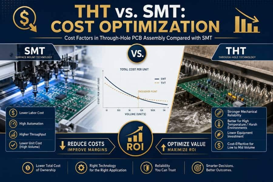
Surface‑mount technology (SMT) and through‑hole technology (THT) each have different cost profiles and strengths.
Automated SMT reflow is generally the most cost‑effective choice for modern, high‑density designs and larger runs, thanks to high placement speeds and the absence of drilling for component leads.
THT offers superior mechanical strength for connectors, high‑current parts, and rugged environments, but per‑joint costs tend to be higher due to drilling, wave or selective soldering, and more manual intervention.
In low cost PCB assembly strategies, a common approach is to reserve THT for parts that truly need mechanical robustness or special behaviour, and handle the rest via SMT whenever possible.
This reduces the number of wave, selective, or manual soldering steps—as well as rework on those operations—and lets more of the build flow through automated SMT lines, which are usually more efficient for cost and throughput.
Mixed‑technology designs (SMT + THT) can still be cost‑effective when processes are sequenced carefully: for example, SMT reflow on one or both sides, followed by wave or selective soldering for carefully grouped THT regions, rather than scattering through‑hole parts all over the board.
Early process planning with your assembly partner—before locking down connector placement and mechanical features—helps identify a flow that meets technical requirements without adding unnecessary steps.
Choosing Practical Inspection Levels
Inspection and testing are essential for catching defects before they become field failures, but not every board needs every test.
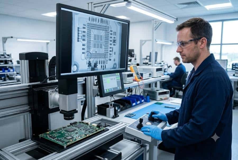
Common inspection and test methods include visual inspection, automated optical inspection (AOI), X‑ray inspection for hidden joints, in‑circuit testing (ICT), flying probe testing, and functional testing.
For early prototypes and low‑risk boards, visual inspection plus AOI can often provide sufficient coverage at relatively low cost, especially when combined with good DFM and design‑rule checks.
In contrast, projects with BGA packages, safety‑critical functions, or high reliability requirements usually justify X‑ray for hidden joints, ICT or flying probe for electrical coverage, and functional tests to validate real‑world behaviour—even though these add to the assembly budget.
Guides on PCB quality control increasingly emphasize that inspection methods should match the product’s risk level and application, rather than being applied uniformly to every board.
From a low‑cost standpoint, this means defining quality expectations clearly, then selecting a combination of AOI, visual checks, limited X‑ray, and targeted electrical tests that gives acceptable confidence without paying for unnecessary depth of coverage on low‑risk builds.
When It Makes Sense to Spend More on Testing
There are scenarios where pushing for the lowest possible test cost is counterproductive. Cheap PCB assembly that skimps on testing can lead to hidden costs such as rework, inconsistent SMT quality, unreliable component sourcing outcomes, and increased failure rates in the field.
For safety‑critical electronics, medical devices, industrial control systems, or high‑volume consumer products with strict return policies, more comprehensive testing (ICT, functional tests, and burn‑in where appropriate) often saves money in the long run by preventing expensive recalls and warranty issues.
In a well‑planned low cost PCB assembly strategy, the goal is therefore not “minimal testing,” but “appropriate testing”: investing more in test coverage when the risk profile and business impact of failure justify it, and using lighter but still structured inspection for lower‑risk prototypes or internal tools.
This risk‑based approach keeps cost aligned with project needs, supporting both affordability and reliability rather than sacrificing one for the other.
When Low Cost PCB Assembly Is the Right Choice
Low cost PCB assembly is most effective when project stage, risk level, and budget priorities line up with what a cost‑conscious manufacturing approach can realistically deliver.
It works best where learning, iteration, and budget efficiency matter more than squeezing the last fraction of performance out of a fully optimized, high‑volume production line.
Prototype and Engineering Builds
Early‑stage projects—prototypes, engineering samples, and development boards—are a natural fit for low cost PCB assembly.
At this stage, designs are often still evolving, market demand is uncertain, and teams need multiple iterations to validate functionality and make informed changes before freezing the layout.
Using cost‑conscious assembly methods here allows you to build more boards, test more ideas, and refine hardware with less budget pressure, while still relying on professional processes and practical inspection to keep prototypes representative of future production hardware.
For startups, university labs, and R&D teams, low cost PCB assembly can be the difference between one hurried prototype and several well‑tested revisions.
Low‑Volume Production Orders
Low‑volume PCB assembly—small batches from a handful of units up to a few hundred—is another area where low cost strategies make strong sense.
In these scenarios, designs typically work but are not fully frozen, or demand is intentionally limited while the market response is still being gauged.
Industry guidance suggests choosing low‑volume assembly when you need flexibility to refine and de‑risk before committing to scale, value quick iterations, and want to avoid large inventory cost while still supplying real customers or internal stakeholders.
Applying low cost assembly principles here—simplified BOMs, efficient panelization, appropriate testing—helps keep per‑unit costs under control without sacrificing the learning and feedback that low‑volume production is meant to provide.
Cost‑Sensitive Turnkey Projects
Full or partial turnkey PCB assembly projects, where the assembler handles both component sourcing and board build, can also benefit from a low cost approach when overall budget and coordination overhead are major concerns.
For small teams and remote customers, turnkey low cost PCB assembly often reduces hidden costs: fewer separate suppliers to manage, consolidated shipping, and one point of contact for BOM issues and DFM questions.
In these cases, the right move is to combine turnkey convenience with the low cost methods discussed earlier—standard components, clear alternates, efficient panelization, and risk‑based inspection—so that total project cost is reduced without relying on the cheapest possible materials or minimal quality checks.
Turnkey low cost PCB assembly is especially attractive for cost‑sensitive products, pilot runs, and geographically distributed teams that prefer a single manufacturing partner to handle logistics and assembly.
Practical Checklist Before Requesting Low Cost PCB Assembly
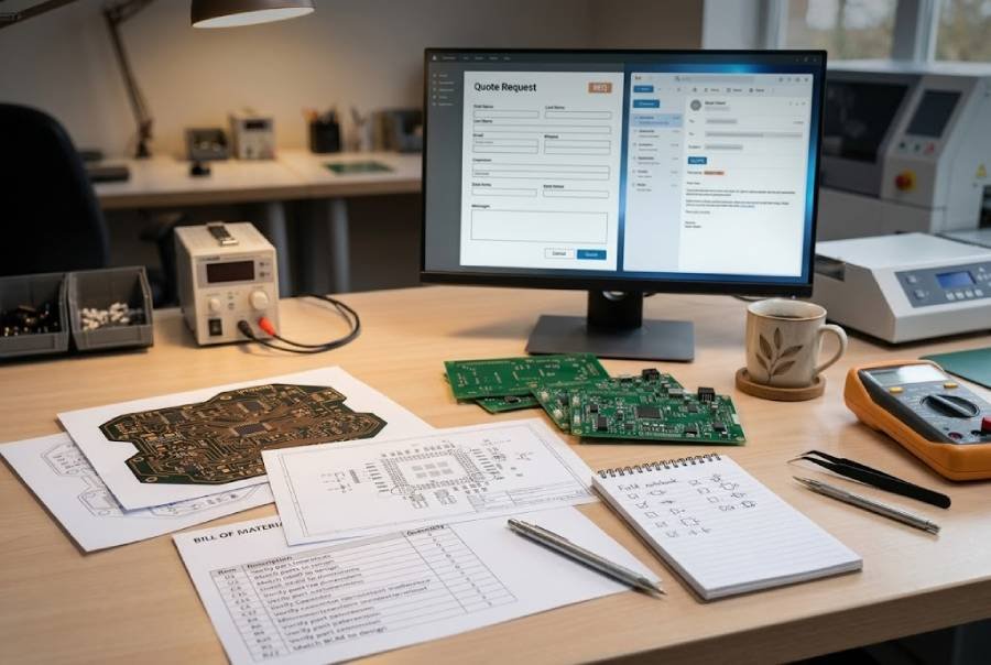
Before you send files for a low cost PCB assembly quote, a short, practical checklist can help make sure your project is ready for cost‑conscious manufacturing and a smooth quotation process.
Preparing the right information up front reduces back‑and‑forth, avoids misalignment between design and expectations, and gives your assembler a clearer basis for suggesting cost‑saving options that still respect reliability requirements.
1. Confirm Design and DFM Readiness
- Board stack‑up, layer count, size, outline, and any special mechanical features are defined and consistent across your design and fab notes.
- Basic DFM checks have been run: trace/spacing, drill sizes and annular rings, solder mask clearances, copper balance, and component keep‑outs around edges and mounting features.
- Panelization intent is at least roughly defined (single boards vs panels), especially for low‑volume runs where panel efficiency can have a big impact on cost.
2. Prepare a Clean, Complete BOM
- BOM is in a structured format (typically Excel/CSV) and includes reference designators, quantities, manufacturer part numbers, descriptions, package types, and any alternates or DNP items.
- Component selections favour widely available, multi‑sourced parts rather than obsolete or single‑source items, and you have indicated where substitutions are acceptable.
- Grouping of identical parts is clear (same MPNs on one line with all associated designators), which simplifies kitting and helps avoid quoting errors.
3. Gather PCB and Assembly Files
- Gerber or ODB++ files are ready, including all copper layers, solder mask, silkscreen, drill data, and a clear board outline.
- Assembly drawings include key notes on component orientation, polarity marks (especially for LEDs and polarized parts), mechanical hardware, labels, and any critical mounting instructions.
- If available, centroid (pick‑and‑place) data and a “golden sample” or reference image can further speed programming and reduce non‑recurring engineering (NRE) charges.
4. Clarify Order Type, Quantities, and Timing
- You’ve categorized the project as prototype, low‑volume, or cost‑sensitive turnkey, and specified how many units you need now and potentially in follow‑up runs.
- Target lead time is defined—standard, quick‑turn, or expedited—so assemblers can quote accordingly and flag where certain cost‑saving methods (like panelization) are more effective.
- Any special compliance requirements (RoHS/lead‑free, IPC class, ITAR/EAR, etc.) are documented so they can be factored into process and cost choices from the start.
5. Specify Testing and Inspection Expectations
- You’ve indicated which inspection and test methods you expect: AOI, X‑ray for BGAs and bottom‑terminated components, flying probe, ICT, functional testing, or first‑article inspection where needed.
- The level of testing you request matches the project’s risk profile—lighter coverage for internal prototypes and more comprehensive testing for safety‑critical or high‑reliability boards.
- Any unique requirements (firmware programming, burn‑in, custom functional jigs, or specific reporting formats) are listed so they can be included in the quote rather than added piecemeal later.
With this checklist in place, it becomes much easier to request low cost PCB assembly in a way that is both realistic and efficient: you give assemblers enough information to apply DFM, propose cost‑saving options, and quote accurately, while keeping reliability expectations clear from the outset.
Bringing Low Cost PCB Assembly Into Your Next Project
Low cost PCB assembly works best when it is treated as a structured set of practices—DFM‑aware design, simplified and sourcing‑friendly BOMs, appropriate process planning, and risk‑based inspection—rather than as a purely price‑driven decision.
By applying these methods during design and preparation, engineering teams and buyers can cut unnecessary assembly expenses while still keeping the reliability and manufacturability of their boards in focus.
For prototypes, low‑volume runs, and cost‑sensitive turnkey projects, this approach often means more iterations, better learning, and a smoother path to scale, without having to accept “cheap” workmanship or opaque sourcing practices.
Ready to apply these low cost PCB assembly methods to a real project?
When your BOM, PCB files, quantities, and testing expectations are ready, you can send them to our Low Cost PCB Assembly Service page to request a cost‑conscious quote for prototype, low‑volume, or turnkey builds.