
Table of Contents
Fine-pitch and micro BGA packages make high-density products possible, but they also narrow the manufacturing window. As pitch shrinks, solder volume, placement tolerance, pad design, reflow behavior, and inspection capability all become more critical, so the same process settings that work for standard BGA parts may no longer deliver stable yield.
For OEM teams, the practical issue is not whether micro BGA can be assembled, but whether the board, package, and process were designed together. A reliable outcome usually depends on coordinated DFM review, tighter stencil and placement control, stronger inspection planning, and realistic expectations about rework risk.
Why Fine-Pitch and Micro BGA Are Different
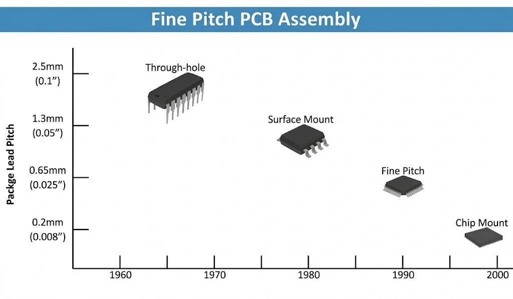
Fine-pitch and micro BGA devices reduce interconnect spacing to support more I/O in less area, but that density removes margin across the entire assembly flow. Around 0.65 mm pitch, routing density rises enough that breakout strategy becomes more demanding, and at about 0.5 mm pitch and below, HDI features such as microvias or more advanced via strategies often become necessary.
Smaller solder balls also mean less solder volume and less forgiveness. When the joint is tiny, even small variation in solder paste release, package coplanarity, pad definition, or reflow balance can cause opens, bridging, or unreliable joints that are difficult to detect visually.
Placement Accuracy and Alignment Risks
Placement accuracy becomes one of the first serious constraints in micro BGA assembly because there is very little room for offset. Although surface tension can help self-align a component during reflow, that effect becomes less forgiving as pitch and solder ball size decrease, especially when paste volume or pad wetting is inconsistent.
In practice, alignment risk comes from several stacked variables: PCB dimensional stability, fiducial quality, machine calibration, nozzle selection, vision alignment, and the condition of the component itself. Industry guidance for fine-pitch placement emphasizes the need for local fiducials near critical areas, controlled placement speed, and process verification before volume release.
Design decisions also influence placement success. Escape routing, copper balance, and nearby component keep-out can affect thermal behavior and available assembly margin, which is why this section should internally link to future content on fine-pitch placement, fanout, and routing best practices.
Solder Paste, Stencil, and Reflow Control
Fine-pitch BGA assembly often succeeds or fails at the solder paste stage. Small apertures are more sensitive to paste particle size, stencil thickness, release efficiency, and aperture design, so insufficient or inconsistent deposit volume can quickly translate into opens, while excess deposit can drive bridging.
For tighter-pitch packages, published process guidance commonly recommends finer powder grades, careful stencil optimization, and solder paste inspection to catch volume drift early. One practical reference notes 25–45 μm powder for pad spacing at or below 0.5 mm, stencil openings around 80–90% of pad size, and routine SPI use to verify height and volume before placement.
Reflow then has to complete the job without introducing new defects. Fine-pitch BGAs are more sensitive to ramp rate, peak temperature, and time above liquidus because the solder joints are smaller and the package may warp more easily; overly aggressive heating can damage the package or accelerate oxidation, while insufficient heat leaves poor coalescence.
Warpage, Bridging, and Head-in-Pillow
As package size, board construction, and thermal loading interact during reflow, warpage becomes a major reliability threat. If the package and PCB do not remain sufficiently planar, some solder balls may separate from the molten paste at the wrong moment, creating opens or the well-known head-in-pillow defect.
Head-in-pillow is especially problematic because it can look acceptable from the outside while hiding incomplete coalescence inside the joint. Design factors such as pad geometry, mask opening, via treatment, copper symmetry, and finish selection all influence this risk, and several recommendations point toward consistent NSMD pad design, filled or capped vias when used in-pad, and balanced thermal conditions across the array.
Bridging and shorting are another concern when solder volume, pad spacing, and reflow wetting are not properly balanced. In dense arrays, the safest strategy is to treat defect prevention as a combined design-and-process problem rather than assuming inspection will catch everything later.
Inspection Limits: AOI, X-Ray, and Test Strategy
Inspection becomes harder as pitch shrinks because the joints are hidden under the component body. AOI remains useful for checking surrounding features, polarity, and some placement conditions, but it cannot directly evaluate most BGA solder joints, which is why X-ray inspection is so important for fine-pitch packages.
X-ray can reveal voids, shorts, opens, solder ball distortion, and some forms of head-in-pillow that would otherwise escape detection. For more demanding diagnosis, 3D CT systems provide deeper visibility than 2D imaging, though they also come with trade-offs in speed and cost.
A practical quality plan therefore combines methods rather than relying on one tool. For critical boards, that can mean SPI before placement, AXI after reflow, and electrical validation such as boundary scan or functional testing before shipment.
DFM for Routing and Via Strategy
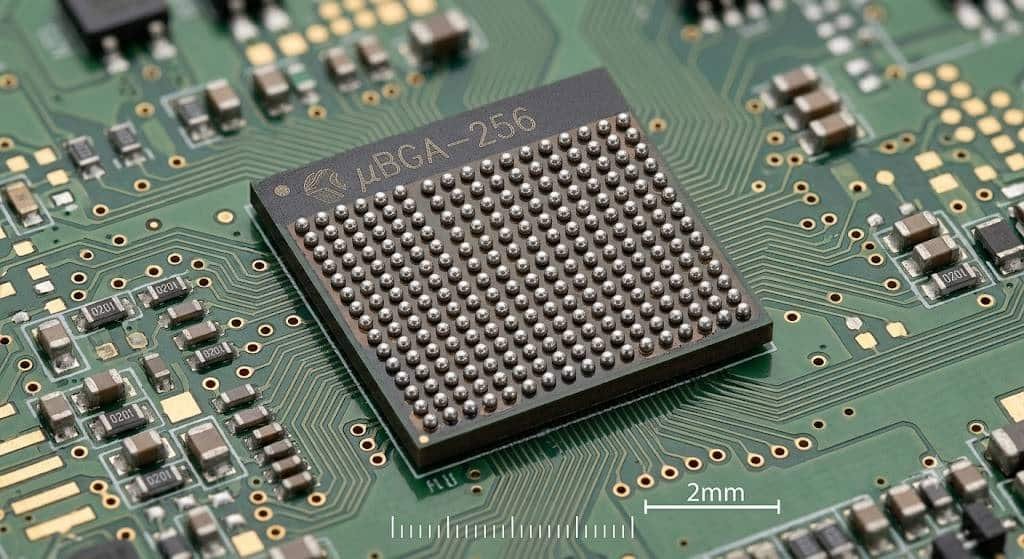
Micro BGA assembly problems often begin in layout rather than on the SMT line. Once pitch drops, fanout strategy, trace width and spacing, via diameter, solder mask clearance, and pad type can determine whether the design is manufacturable at all.
At finer pitch, dog-bone breakout may no longer be enough, and HDI structures such as microvias, blind vias, buried vias, or via-in-pad can become necessary. When vias are placed in-pad, guidance consistently points to filled and capped structures to avoid solder loss, non-planar pads, and wetting-related defects.
Design teams should also watch copper balance and thermal symmetry. Uneven copper attachment, large direct plane connections, and inconsistent pad environments can raise the probability of uneven heating and head-in-pillow, especially near the corners and edges of the package.
Rework Risk and Repair Limits
Rework is possible for many BGA packages, but the economics and technical risk become less favorable as pitch decreases. Removing and replacing a micro BGA demands tightly controlled heating, accurate site preparation, careful alignment, and post-rework validation, and every cycle adds stress to pads, laminate, and nearby components.
The main concern is not only whether the part can be replaced, but whether the board remains trustworthy afterward. Heat shields, staged thermal profiles, professional rework stations, and thorough post-rework inspection are commonly recommended to protect adjacent parts and confirm the integrity of the repaired site.
For many high-reliability products, the smarter strategy is to prevent rework through better NPI validation, stencil tuning, and DFM review before volume production. That idea deserves an internal link to any future BGA rework guide as well as to service pages covering NPI and pilot runs.
Best Practices for Stable Yield
Stable yield in fine-pitch and micro BGA assembly usually comes from process discipline rather than one special trick. The strongest programs combine early DFM review, moisture control, solder paste verification, accurate placement, controlled reflow, X-ray-based inspection, and clear acceptance criteria tied to the product’s reliability class.
A useful rule is to treat the package, PCB, and process as one system. When designers share stack-up, via strategy, pad design, and thermal details early, the assembly team can tune stencil design, profile settings, and inspection points before problems reach production.
For customers evaluating an assembly partner, the most valuable questions are practical ones: What pitch can be built consistently, what inspection method is used for hidden joints, how are via-in-pad designs handled, and how is rework qualified? Those answers reveal far more about real capability than a generic capability list.
Process Checklist
The checklist below can be offered as a downloadable template for engineers and sourcing teams before releasing a fine-pitch or micro BGA build.
| Checkpoint | What to Confirm | Why It Matters |
|---|---|---|
| Package review | Pitch, ball size, MSL rating, coplanarity requirements | Confirms assembly difficulty and moisture handling needs. |
| PCB design review | Fanout method, via-in-pad treatment, mask clearance, copper balance | Prevents solder loss, warpage sensitivity, and routing-driven defects. |
| Stencil review | Aperture reduction, thickness, paste type, SPI plan | Controls paste volume and print consistency. |
| Placement review | Fiducials, nozzle choice, machine capability, keep-out area | Reduces offset and placement-related failures. |
| Reflow review | Ramp rate, peak temperature, TAL, atmosphere | Balances wetting, warpage control, and joint formation. |
| Inspection review | AOI scope, X-ray criteria, electrical test coverage | Addresses hidden-joint verification limits. |
| Rework review | Rework criteria, tooling, post-rework inspection | Sets realistic repair expectations and protects reliability. |
Fine-pitch and micro BGA assembly is manageable, but only when design and manufacturing are aligned from the start. The closer the pitch, the less room there is for assumptions, which is why detailed DFM review and hidden-joint inspection should be treated as baseline requirements rather than optional upgrades.