
Table of Contents
Understanding BGA Assembly and Its Challenges
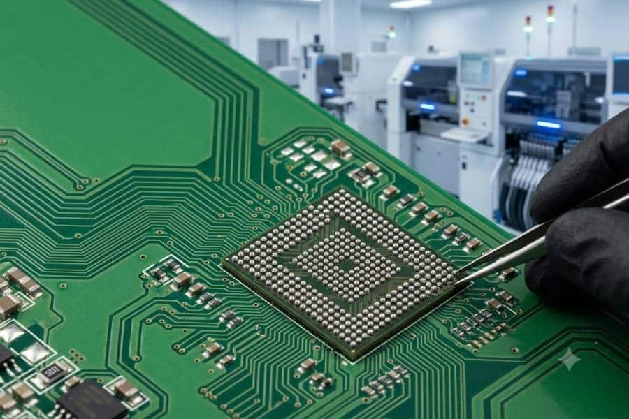
Ball Grid Array (BGA) packages are widely used in modern electronics because they offer high I/O density in a compact footprint and excellent electrical performance for high‑speed signals. Instead of using traditional gull‑wing leads, BGAs rely on an array of solder balls underneath the package to connect to the PCB pads, which allows more connections in a smaller area and simplifies routing for complex processors, FPGAs, and communication chips.
For a practical overview of our BGA PCB assembly capabilities and typical applications, you can refer to our dedicated BGA PCB Assembly services page on pcbelec.com.
If you want to start with a more general introduction before diving into the step‑by‑step process, you can also read our first article on BGA PCB assembly basics and benefits.
Pre‑assembly Preparation
Before any BGA component is placed on the PCB, proper pre‑assembly preparation is essential to avoid defects that are difficult or impossible to repair later. This preparation includes both PCB design considerations and handling procedures for moisture‑sensitive BGA devices.
On the PCB design side, the pad layout and surrounding routing must match the BGA package and assembly capability. Designers need to define pad sizes and solder mask openings that support stable solder‑ball wetting, avoid excessive solder bridging, and minimize voids. Escape routing under the BGA—using microvias, via‑in‑pad filled and capped vias, or blind/buried vias—should be planned to balance signal integrity, manufacturability, and cost. If the design pushes very fine pitch BGAs, it is important to confirm with the assembly house that their stencil printing, placement, and reflow processes can reliably handle the chosen geometry.
On the component side, most BGAs are classified as moisture‑sensitive devices and follow JEDEC MSL (Moisture Sensitivity Level) handling guidelines. Improper storage or exposure to humidity can cause internal moisture to expand rapidly during reflow, leading to package cracking or “popcorn” failures. To prevent this, BGA components must be stored in dry conditions, tracked for floor life, and baked according to the manufacturer’s recommendations when necessary. Clear procedures for incoming inspection, packaging opening, baking, and material flow on the shop floor help keep BGA devices within their specified limits and reduce latent reliability risks.
By treating PCB design and component handling as part of the same pre‑assembly preparation stage, manufacturers build a more robust foundation for the subsequent BGA assembly steps. Good communication between design engineers, process engineers, and buyers at this early stage often prevents expensive redesigns or rework later in the project.

Stencil Design and Solder Paste Printing
Stencil Design for BGA Pads
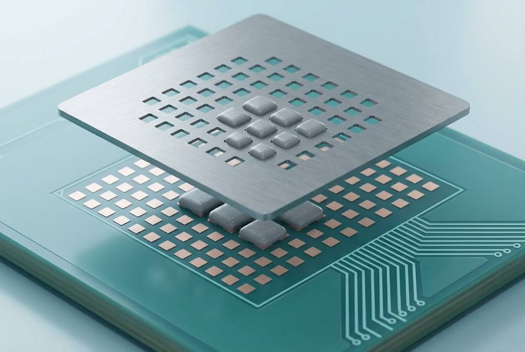
For BGA assembly, stencil design directly influences the volume and shape of solder deposited on each pad, which in turn determines joint quality after reflow. The stencil thickness, aperture size, and aperture shape must be carefully matched to the BGA pitch, pad diameter, and overall board design.
Thinner stencils help control solder volume for fine‑pitch BGAs, reducing the risk of bridging and improving wetting consistency. However, if the stencil is too thin, it may not provide enough solder for larger components on the same board. In such mixed‑technology designs, step stencils or local thickness reductions are often used to balance the needs of BGAs and other components. Aperture reductions—such as making the opening slightly smaller than the pad or using rounded or “windowed” shapes—can further optimize paste release and reduce void formation in the final joints.
Solder Paste Selection and Printing Parameters
Solder paste selection is another critical factor in BGA assembly quality. The alloy composition must match the product requirements (for example, lead‑free SAC alloys versus traditional leaded formulations), while the powder size must be suitable for the BGA pitch to avoid clogging and ensure smooth deposition. For fine‑pitch BGAs, smaller particle sizes typically provide more stable printing through small apertures, but require tighter control of storage and handling.
During printing, parameters such as squeegee speed, pressure, and separation speed affect how well solder paste fills and releases from the stencil apertures. Consistent environmental conditions—temperature, humidity, and paste age—also help maintain stable viscosity and prevent defects like insufficient solder, smearing, or bridging. Well‑defined printing process windows, combined with regular stencil inspection and cleaning, are essential to ensure that every BGA pad receives the right amount of solder paste before placement.
For designs that push very fine‑pitch BGAs or complex escape routing, our engineering team at PCBELEC can review your PCB layout and assembly requirements and suggest practical improvements. You can submit your files and requirements directly through our BGA PCB Assembly services page.
BGA Placement
Pick‑and‑Place Accuracy and Vision Alignment
After solder paste printing, accurate placement of BGA components is crucial for forming reliable joints during reflow. Modern pick‑and‑place machines use high‑resolution vision systems to locate fiducials on the PCB and align each BGA package to its pad array. This ensures that the solder balls sit within the correct tolerance window relative to the pads, even for very fine‑pitch devices.
Placement accuracy is defined not only by the machine’s mechanical capability, but also by the stability of the PCB support, nozzle design, and component presentation. Warped boards, worn nozzles, or inconsistent tape‑and‑reel feeding can all lead to small shifts in position or rotation that may cause opens or shorts after reflow. For BGAs, even minor misalignment can result in partial contact between balls and pads, making process control and regular maintenance of equipment especially important.
Typical BGA Placement Defects and Their Causes
Common placement‑related defects in BGA assembly include offset components, rotation errors, and variations in height or coplanarity. If a BGA is significantly offset, some solder balls may not land on their pads at all, leading to open circuits. Rotation errors are particularly critical because they can misplace entire groups of balls and cause multiple shorts or opens.
Coplanarity issues occur when the package or PCB is not flat, causing uneven contact between solder balls and paste deposits. Combined with inconsistent paste volumes, this can contribute to defects such as head‑in‑pillow, where the solder ball and paste fail to properly merge during reflow. To minimize these risks, manufacturers control board support tooling, verify package quality from suppliers, and optimize placement force and speed parameters for BGA devices.

Reflow Soldering Profile for BGA
Key Zones in the Reflow Profile
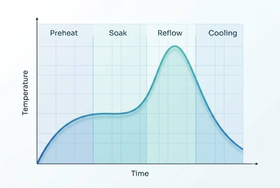
The reflow soldering profile defines how temperature changes over time as the PCB with BGAs passes through the oven, and it plays a central role in creating reliable solder joints. A typical profile includes preheat, soak (or thermal equilibrium), reflow, and cooling stages, each with specific targets for temperature and ramp rate.
During preheat, the board and components are gradually brought up to temperature to avoid thermal shock and to activate flux in the solder paste. The soak stage helps equalize temperatures across the assembly and drives off solvents, which is particularly important for dense BGA areas where heat distribution can be uneven. In the reflow stage, the temperature rises above the alloy’s liquidus point long enough for solder balls and paste deposits to fully melt and wet the pads. Controlled cooling then promotes proper grain structure and reduces the risk of micro‑cracking or warpage.
Lead‑Free vs. Leaded BGA Reflow Considerations
Lead‑free BGA assemblies typically require higher peak temperatures than leaded ones, which increases stress on components and the PCB. Manufacturers must ensure that the chosen profile stays within the thermal limits specified by both the BGA package and the board materials. Excessively high temperatures or rapid heating can contribute to defects such as warpage, head‑in‑pillow, and voids in the solder joints.
To optimize BGA reflow, process engineers monitor factors such as maximum peak temperature, time above liquidus, and temperature uniformity across different board locations. Using thermocouples attached near or under BGA areas, they validate that the actual profile matches the target and adjust conveyor speed, zone temperatures, and airflow settings as needed. A stable, well‑characterized profile reduces variability and helps ensure that every BGA joint reaches the correct temperature window for proper soldering.
Inspection – X‑ray, AOI and Functional Test
X‑ray Inspection for Hidden BGA Joints
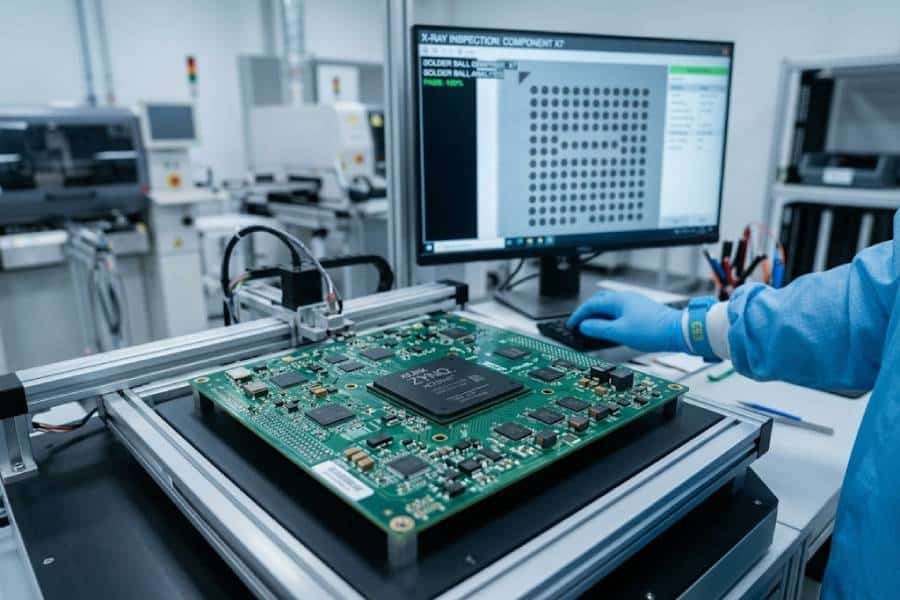
Because BGA solder joints are located under the package and cannot be seen directly, X‑ray inspection is the primary method used to evaluate their quality. X‑ray systems generate images that reveal the shape, position, and internal structure of the solder balls and joints, allowing engineers to spot defects that would otherwise remain invisible.
Typical BGA defects detected by X‑ray include voids inside the solder joints, opens where a ball fails to connect to the pad, and shorts caused by unintended solder bridges. X‑ray can also highlight misalignment, insufficient solder, and head‑in‑pillow defects, where the ball and paste do not fully merge. By analyzing these images, process engineers fine‑tune stencil design, printing parameters, placement accuracy, and reflow profiles to improve overall assembly quality.

AOI and Electrical/Functional Testing
Automated Optical Inspection (AOI) complements X‑ray by checking visible features such as component presence, polarity, and solder fillets around non‑BGA devices. While AOI cannot see BGA joints under the package, it helps catch other assembly issues that might affect the product’s performance or reliability. Together, AOI and X‑ray provide a more complete view of the assembly quality.
Electrical and functional tests, such as ICT (In‑Circuit Test) and FCT (Functional Circuit Test), verify whether the assembled board works as intended in real operating conditions. These tests can detect latent issues that are not obvious in visual or X‑ray inspection, such as intermittent connections or performance problems under load. For products that rely heavily on BGAs—like processors, memory, and complex communication modules—combining X‑ray, AOI, and robust electrical testing is essential to build confidence in long‑term reliability.
To learn more about how we combine X‑ray inspection, AOI, and electrical testing in real production projects, visit our BGA PCB Assembly services page where we outline our quality‑control approach and typical test strategies for high‑density boards.
BGA Rework and Repair Process
When and Why BGA Rework Is Needed
Even with a well‑controlled process, some BGAs may need to be reworked due to defects, design changes, or component issues. Because BGAs are expensive and often critical to product functionality, rework allows manufacturers to salvage boards instead of scrapping entire assemblies. However, reworking BGAs is technically challenging and must be handled carefully to avoid damaging the PCB or nearby components.
Common reasons for BGA rework include X‑ray‑identified defects such as opens, shorts, or excessive voids, as well as component failures discovered during functional testing. In some cases, design updates or firmware changes may require replacing a processor, memory device, or other BGA component with a newer revision. Understanding when rework is feasible and when a board should be scrapped is part of overall process and cost management.
Typical BGA Rework Steps
A standard BGA rework process starts with controlled removal of the existing component using a dedicated rework station. The station applies localized heating to bring the solder joints above reflow temperature while protecting the rest of the board. Once the BGA is lifted, residual solder and flux are carefully cleaned from the pads to prepare a flat, contamination‑free surface for the new device.
If the removed BGA is to be reused, it may need to be reballed—replacing the original solder balls with new ones using a stencil and controlled reflow. The new or reballed component is then aligned and placed onto the PCB, often with fresh solder paste or flux, and subjected to a reflow profile optimized for rework conditions. Throughout this process, strict control of temperature, alignment, and handling is essential to avoid pad damage, solder mask lifting, or internal component stress. Proper documentation and limits on the number of rework cycles help maintain reliability over the product’s lifetime.
How PCBELEC Ensures Reliable BGA Assembly
Process‑Driven Control Across Every Step
Reliable BGA assembly depends on how consistently each process step is executed—from pre‑assembly preparation to printing, placement, reflow, inspection, and potential rework. pcbelec focuses on defining clear process windows and documenting best practices for BGA handling, so that engineers and operators follow the same standards on every batch. This includes design reviews for BGA pad and via structures, stencil optimization for fine‑pitch packages, and validated reflow profiles tailored to the specific solder alloy and board stack‑up.
By combining experienced engineering support with stable equipment and materials, pcbelec aims to minimize common BGA defects such as voids, opens, shorts, head‑in‑pillow, and warpage‑related issues. Feedback from X‑ray inspection, AOI, and electrical testing is used to continuously refine stencil design, printing parameters, placement accuracy, and oven settings.
A more detailed description of our equipment, minimum BGA pitch capability, and typical industries served is available on our BGA PCB Assembly services page.
If you are planning a new project that involves BGA‑rich designs and need a manufacturing partner, you can submit your BOM and Gerber files through that page to receive a tailored quotation and process review from our engineering team.
Inspection, Testing and Engineering Support for Customers
In addition to process control, pcbelec relies on comprehensive inspection and test coverage to build confidence in BGA PCB assemblies. X‑ray inspection is applied to critical BGA devices to verify joint quality, while AOI checks the rest of the SMT population for placement and soldering issues. Where needed, ICT and functional tests are used to confirm that the assembled boards perform correctly under real‑world operating conditions.
For customers, PCBELEC provides engineering support during design and prototype stages to help align BGA layout, stencil strategy, and assembly capability. Early communication on topics such as via‑in‑pad, minimum BGA pitch, and test coverage can reduce the risk of redesigns and speed up the transition from engineering samples to stable mass production. By treating BGA assembly as a collaboration between design, manufacturing, and test, PCBELEC works to deliver boards that meet both performance and reliability expectations.