
Table of Contents
BGA soldering defects often stay hidden under the package, which means they can look fine from the outside while still creating reliability problems underneath. In this article, we’ll focus on the defects that matter most in real production, what usually causes them, and how to prevent them before they reach the field.
Why BGA defects matter
Ball Grid Array assemblies are widely used in high-density electronics because they support compact layouts and strong electrical performance, but the solder joints are not visible after reflow. That hidden-joint structure makes BGA process control and inspection especially important, since defects such as opens, shorts, voids, and head-in-pillow can be difficult to catch without X-ray inspection.
What this article covers
This guide breaks down the most common BGA soldering defects, explains why they happen, and shows practical ways to reduce risk through stencil control, placement accuracy, reflow optimization, and post-reflow inspection. It is written for engineers and buyers who want a clearer view of how to improve yield and avoid costly rework later in the process.
What Makes BGA Soldering Difficult
BGA soldering is difficult because the solder joints are hidden under the package, so many problems cannot be confirmed by simple visual inspection. The process is also sensitive to stencil design, paste volume, placement accuracy, reflow profile, board warpage, and moisture control, which means small process variations can create hidden defects that are hard to rework later.
What makes it difficult
Unlike many other SMT packages, a BGA does not expose its solder joints around the edge, so engineers often need X-ray or other advanced inspection methods to evaluate the joint quality after reflow. That hidden structure makes BGA assemblies more dependent on process discipline, because the assembly process determines joint integrity more than inspection does.
Process sensitivity
BGA soldering is especially sensitive to the balance between solder paste amount, thermal profile, and component placement. If the paste volume is too high or the stencil design is off, bridging can occur; if wetting is incomplete or warpage is present, defects like head-in-pillow or open joints can appear. Board warping, oxidation, and insufficient thermal control can also increase the risk of non-wetting and weak joints.
Why this matters
This is why BGA assembly usually requires tighter process windows than simpler packages, especially in high-density or high-reliability products. In practical terms, good BGA results depend on controlling the process before defects happen, not just detecting them afterward.

Common BGA Soldering Defects
BGA soldering defects usually fall into a few recurring categories: solder bridging, voids, head-in-pillow, open joints or non-wetting, and misalignment-related defects. Because the joints are hidden beneath the package, these problems are often not visible from the outside and usually need X-ray inspection or other advanced methods to confirm.
Common defect types
- Solder bridging happens when excess solder creates an unintended connection between adjacent balls, which can lead to shorts and immediate electrical failure.
- Voids are trapped gas pockets inside the solder joint; they reduce mechanical strength and can hurt thermal performance, especially in high-power designs.
- Head-in-pillow occurs when the solder ball and solder paste do not fully coalesce during reflow, leaving a weak or incomplete joint that may pass initial checks but fail later under stress.
- Open joints and non-wetting happen when the solder does not properly bond to the pad, often because of insufficient solder, oxidation, contamination, or poor thermal energy during reflow.
- Misalignment can also create weak joints or shorts when the package is not accurately placed on the pad array before reflow.

Root Causes Behind These Defects
BGA soldering defects are usually the result of several process stresses acting together rather than a single isolated mistake. In practice, stencil design, solder paste volume, reflow temperature profile, component warpage, oxidation, contamination, and moisture sensitivity all influence whether the final joint forms correctly or becomes defective.
Root cause groups
1. Stencil and paste issues
Too much or too little solder paste is one of the most common reasons BGA joints fail. If the stencil aperture is oversized, solder can bridge; if the aperture is too small or uneven, the joint may become weak, open, or incomplete. Paste type, print quality, and paste freshness also matter because they affect how much solder and flux are available during reflow.
2. Reflow profile problems
The reflow profile has a direct effect on how well solder balls and paste coalesce. If the board heats too quickly, too slowly, or reaches the wrong peak temperature, the solder may not fully wet, voids may remain trapped, or head-in-pillow defects may form. Large temperature differences across the package can also create uneven melting, especially on larger or more warp-prone BGAs.
3. Warpage and coplanarity
Component or board warpage is a major contributor to head-in-pillow and open joints. When the package flexes during heating, some balls can lose contact with the paste, then re-contact later without fully bonding, which leaves a weak or incomplete connection. Coplanarity problems are especially important on corner balls, where separation is more likely to appear first.
4. Oxidation and contamination
Oxidation on solder balls or PCB pads can block proper wetting, especially when flux activity is not strong enough to remove the oxide layer during reflow. Contamination from residues, moisture, or poor storage can also interfere with bonding and contribute to non-wetting, voids, or head-in-pillow defects.
5. Moisture and handling
Moisture-sensitive components can absorb water during storage or handling, and that moisture may turn into gas during reflow. If the device is not baked or stored correctly, the result can be additional voiding, poor wetting, or other latent reliability issues that may not appear until later in the product life cycle.

How to Prevent BGA Soldering Defects
Preventing BGA soldering defects starts long before reflow. In most cases, stable results come from controlling the full process chain, including PCB design, stencil and solder paste setup, component handling, placement accuracy, thermal profiling, and post-reflow inspection.
One of the first priorities is optimizing solder paste deposition. Stencil aperture size, stencil thickness, and print consistency all affect whether the solder volume is sufficient and uniform across the BGA site, and poor control here can lead to bridging, opens, or weak joints. For void-sensitive designs, some manufacturers also use modified aperture patterns such as window-pane layouts to reduce paste concentration and create channels for gas to escape during reflow.
Material handling is another major prevention step. Because many BGA devices are moisture-sensitive, they need to be stored under controlled humidity and baked when exposure limits are exceeded, otherwise absorbed moisture can contribute to voiding, poor wetting, and latent reliability risks during reflow. Clean pad surfaces, fresh solder paste, and well-controlled oxidation levels also help preserve wetting performance and reduce the risk of head-in-pillow or non-wetting defects.
Placement accuracy must also be tightly controlled. Local fiducials, stable board support, coplanarity checks, and accurate pick-and-place settings help keep each BGA aligned and in proper contact with the paste before the thermal cycle begins. This becomes especially important for fine-pitch packages and larger BGAs, where even small shifts or warpage can increase the chance of opens, shorts, or incomplete coalescence.
Reflow optimization is one of the most effective ways to prevent recurring BGA defects. A controlled ramp rate, an adequate soak period, a suitable peak temperature, and a stable cooling rate all help the solder wet correctly, release trapped volatiles, and limit warpage stress during the molten stage. In more demanding builds, nitrogen reflow and profile tuning across the full board can further reduce oxidation and improve consistency under dense BGA arrays.
Inspection should be treated as part of prevention, not only as a final checkpoint. X-ray inspection, solder paste inspection, and defect trend tracking help manufacturers catch process drift early and adjust stencil design, print quality, or thermal settings before the same issue repeats across a larger batch. That is why high-yield BGA assembly usually depends on closed-loop control rather than one-time troubleshooting after defects appear.
Inspection and Detection Methods
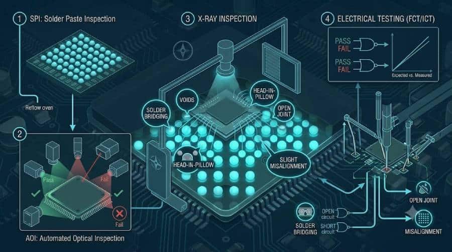
Because BGA solder joints are hidden beneath the component body, inspection methods that work well for gull-wing or leaded packages are not enough on their own. Effective BGA quality control usually depends on combining solder paste inspection, optical inspection, X-ray analysis, and electrical testing so defects can be found at different stages of the assembly process.
Solder Paste Inspection, or SPI, is often the first useful checkpoint. It verifies whether the solder paste deposits on the BGA pads have the right volume, height, and alignment before placement, which helps catch printing problems before they turn into opens, shorts, or void-related issues after reflow.
Automated Optical Inspection, or AOI, is valuable for checking visible assembly conditions such as missing components, polarity errors, surface bridges, and placement offsets. However, AOI cannot see beneath a BGA package, so it is useful as a complementary method rather than the main tool for judging hidden BGA joint quality.
For BGA assemblies, X-ray inspection is the most important post-reflow method because it can evaluate hidden solder joints without destroying the board. Automated X-ray Inspection, often called AXI, is widely used to detect voids, solder bridging, open joints, missing or displaced balls, and other internal defects that optical inspection cannot confirm. In more advanced cases, manufacturers may use off-axis imaging, laminography, or 3D CT to improve visibility of joint shape, misalignment, and defect location under complex packages or multilayer boards.
Electrical tests add another layer of confidence after visual and X-ray inspection. In-Circuit Test, flying probe, boundary-scan, and functional testing can verify connectivity and product behavior, which helps identify intermittent or performance-related issues that may not be obvious in an image alone. At the same time, electrical tests do not always reveal whether a joint is mechanically robust, so a weak BGA connection may still require X-ray evidence for proper diagnosis.
In practice, the best inspection strategy is staged rather than isolated. SPI helps prevent printing-related defects, AOI screens visible placement problems, X-ray confirms hidden solder joint integrity, and electrical testing verifies that the finished board actually works under operating conditions. This layered approach is especially important for BGA devices because no single inspection method can fully characterize every possible failure mode on its own.
Design and Process Tips for Better Yield
Improving BGA yield starts with design for manufacturability rather than with rework after defects appear. When pad design, via strategy, stack-up planning, stencil setup, and process validation are aligned early, manufacturers have a much better chance of building consistent BGA joints across prototype and production runs.
One of the most important design decisions is the BGA land pattern itself. Pad diameter, solder mask definition, paste opening, and surface flatness all influence how solder wets and collapses during reflow, so these parameters should match both the package specification and the assembler’s process capability. For dense layouts, via-in-pad can help routing and escape design, but it also raises assembly risk unless the vias are properly filled, capped, and planarized.
Stencil and paste design should be treated as part of yield engineering, not just printing setup. Aperture size, stencil thickness, release performance, and print parameters directly affect solder volume consistency, which in turn affects bridging, opens, and voiding risk under BGAs. For tighter pitches, controlled aperture reduction and validation through SPI can help keep paste deposits stable from board to board.
Board support and warpage control are also critical. If the PCB bends during placement or reflow, corner balls and marginal joints become much more vulnerable to head-in-pillow, misalignment, or incomplete collapse, so fixture strategy and thermal uniformity should be reviewed before production ramps. In more demanding applications, minimizing warpage in the BGA area and validating the full board profile can make a noticeable difference in final yield.
A strong yield strategy also depends on process feedback. X-ray inspection, visual checks, paste measurement, and defect trend analysis should feed back into stencil refinement, placement adjustment, and profile tuning instead of remaining isolated quality records. This closed-loop approach helps manufacturers identify whether defects come from printing, placement, materials, or thermal imbalance, which is much more effective than treating every failure as a one-off event.
For engineering teams, one practical rule stands out: do not evaluate BGA yield only at the assembly stage. The best results usually come when PCB design, process engineering, and inspection planning are coordinated from the beginning, especially for fine-pitch, high-pin-count, or high-reliability products.

Conclusion
BGA soldering defects are challenging not because they are impossible to manage, but because many of them develop silently beneath the package and are difficult to confirm without the right process controls and inspection methods. Problems such as bridging, voids, head-in-pillow, and open joints are often linked to the combined effects of design choices, solder paste behavior, placement accuracy, thermal profiling, moisture control, and hidden joint inspection.
That is why reliable BGA assembly depends less on isolated troubleshooting and more on a coordinated manufacturing strategy. When DFM review, stencil optimization, controlled reflow, warpage management, X-ray inspection, and test feedback all work together, manufacturers are far more likely to improve yield, reduce rework, and protect long-term product reliability.