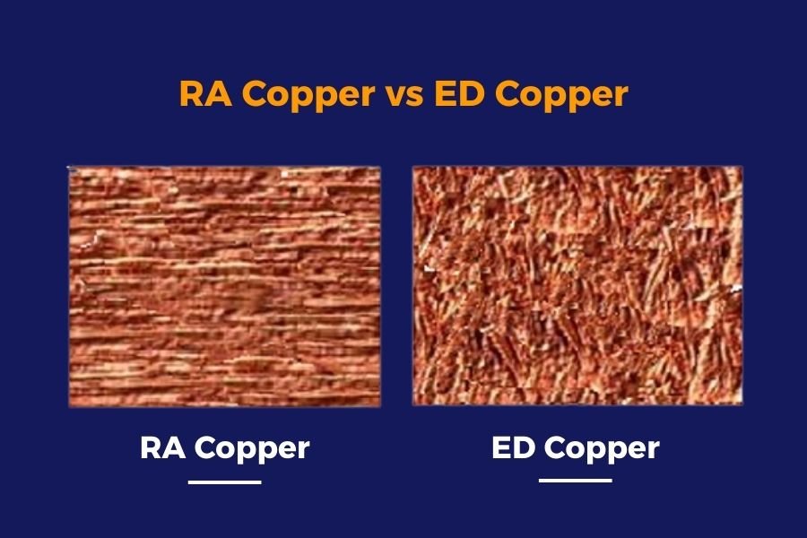
What is a Pad in PCB Design?
What are pads in PCBs and why are they so important for electronics design and manufacturing? This definitive guide covers pad types, layout considerations, and the overarching significance of PCB pads.
Via-in-pad technology for PCBs places vias directly within surface mount pads, conserving space by merging interconnect structures. Learn benefits and reliability factors in applying this innovation.
An Introduction to Via-in-Pad for Printed Circuit Boards Read More »
Filled and capped vias are advanced PCB design techniques that measurably enhance connection reliability. Learn when and why to leverage precision via filling and durable capping to prevent moisture ingress, fractures, and short circuits.
Leveraging Filled and Capped Vias for Enhanced PCB Reliability Read More »
What are tented vias and why should PCB designers use them? Read our full guide covering how tented vias work, their benefits, ideal applications, and how to construct boards with quality via tenting.
What are Tented Vias? A Guide to This Important PCB Feature Read More »
Blind vias and buried vias enable improved signal routing, component density, performance, and simplified PCB stackups essential for complex, high-speed designs. This article explains what blind and buried vias are and key considerations for implementation.
Blind Vias, Buried Vias in PCBs – A Complete Guide Read More »
Vias enable complex functionality in printed circuit boards by facilitating vertical transitions between layers. This article provides an overview of via roles, types, reliability factors, advanced structures, and the ongoing innovation driving PCB performance.
Explore the intricate journey of double-layer PCB manufacturing at JHYPCB, from routing to shipping. Witness the precision of processes like routing, V-cut, and QC, ensuring top-quality PCB fabrication.
Navigating The PCB Manufacturing Process Part 5: Testing, V-cut, QC, And Shipping Read More »
We have now covered initial PCB production processes – substrate preparation, imaging, plating, etching to form circuitry. The board is now a semi-finished product. This section explains solder mask application to shield copper traces, silkscreen printing for informational markings and labels, and surface metal treatments to protect pads from oxidation while promoting soldering. With these enhancements, boards are fully ready for electronics assembly.
Navigating The PCB Manufacturing Process Part 4: Solder Mask, Silkscreen, Surface Finish Read More »
We have covered initial PCB production steps – milling, foil lamination, drilling. Now we detail processes to transform base material into functional printed circuit board. First, copper electroplating deposits into drilled holes and grows copper thickness. Photolithography uses UV light to transfer layout pattern onto copper layer. Exposed copper gets etched away, leaving only desired conductive traces. Finally, automated optical inspection compares board to original design to validate quality.
Navigating The PCB Manufacturing Process Part 3: Pattern And AOI Read More »
In our PCB manufacturing process deep dive, we explored lamination, exposure, and development steps that transfer circuit layouts onto boards. Up next, we tackle graphical electrodeposition and AOI.
Navigating The PCB Manufacturing Process Part 2: Copper Plating, Routing Read More »