Navigating The PCB Manufacturing Process Part 3: Pattern And AOI
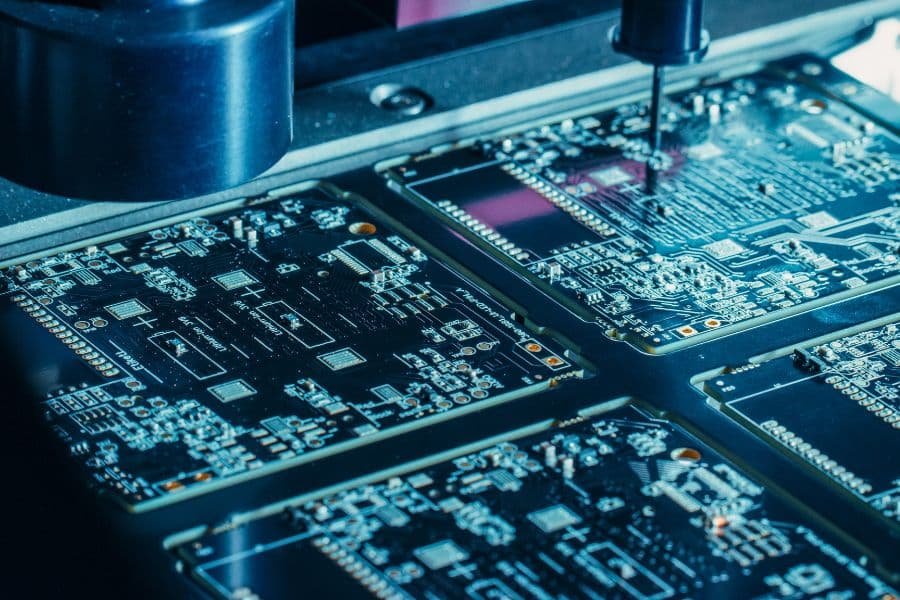
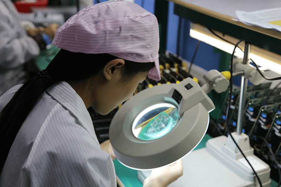
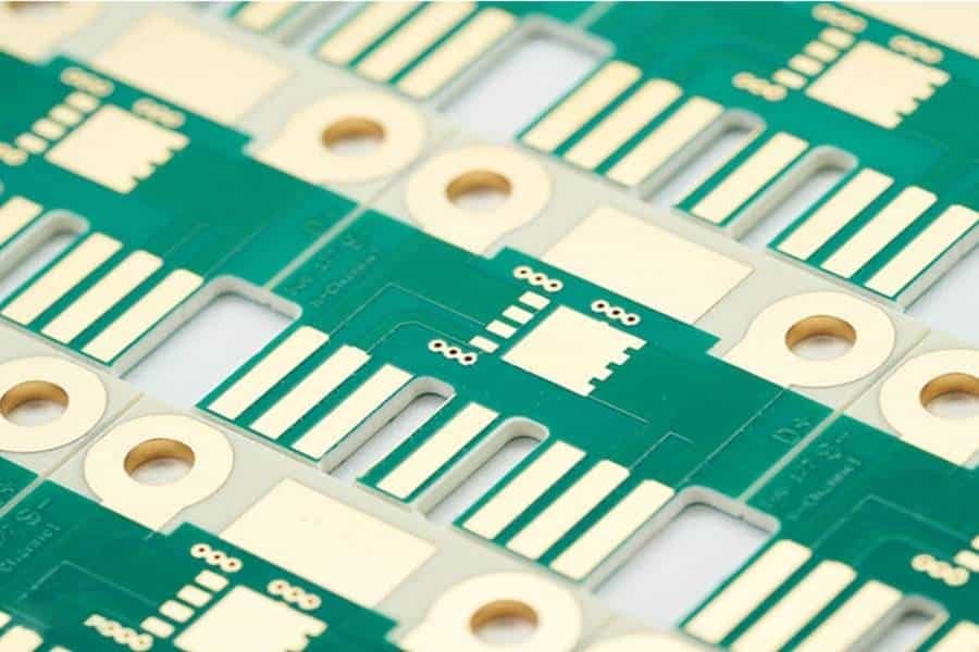
We have covered initial PCB production steps – milling, foil lamination, drilling. Now we detail processes to transform base material into functional printed circuit board. First, copper electroplating deposits into drilled holes and grows copper thickness. Photolithography uses UV light to transfer layout pattern onto copper layer. Exposed copper gets etched away, leaving only desired conductive traces. Finally, automated optical inspection compares board to original design to validate quality.
Navigating The PCB Manufacturing Process Part 3: Pattern And AOI Read More »