


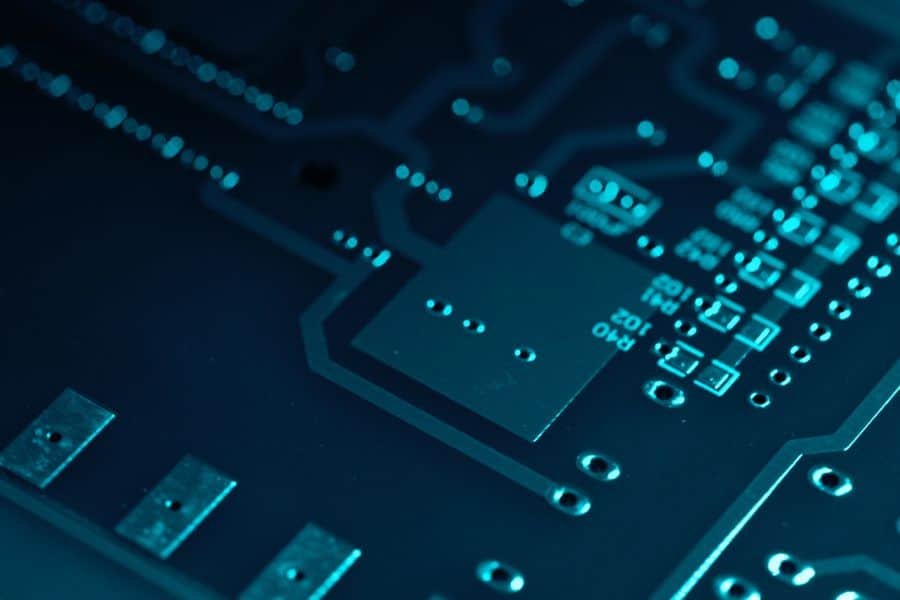
What is a Pad in PCB Design?
What are pads in PCBs and why are they so important for electronics design and manufacturing? This definitive guide covers pad types, layout considerations, and the overarching significance of PCB pads.
What are pads in PCBs and why are they so important for electronics design and manufacturing? This definitive guide covers pad types, layout considerations, and the overarching significance of PCB pads.

Via-in-pad technology for PCBs places vias directly within surface mount pads, conserving space by merging interconnect structures. Learn benefits and reliability factors in applying this innovation.
An Introduction to Via-in-Pad for Printed Circuit Boards Read More »
Filled and capped vias are advanced PCB design techniques that measurably enhance connection reliability. Learn when and why to leverage precision via filling and durable capping to prevent moisture ingress, fractures, and short circuits.
Leveraging Filled and Capped Vias for Enhanced PCB Reliability Read More »
What are tented vias and why should PCB designers use them? Read our full guide covering how tented vias work, their benefits, ideal applications, and how to construct boards with quality via tenting.
What are Tented Vias? A Guide to This Important PCB Feature Read More »
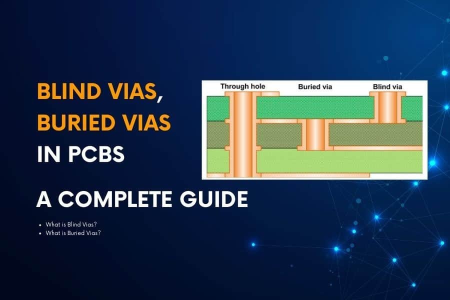
Blind vias and buried vias enable improved signal routing, component density, performance, and simplified PCB stackups essential for complex, high-speed designs. This article explains what blind and buried vias are and key considerations for implementation.
Blind Vias, Buried Vias in PCBs – A Complete Guide Read More »
Plated through holes (PTHs) are vital in printed circuit boards for enabling reliable connectivity between layers. This article explores PTHs in depth—from their key benefits like durable interlayer connections and flexible component placement, to critical design considerations around hole size, spacing, depth. We also contrast PTHs to cheaper non-plated holes, and overview popular alternatives like blind and buried vias and their ideal use cases. For PCB designers and manufacturers, our insights help inform effective PTH integration tailored to your product requirements. Reach out to explore our professional PCB fabrication utilizing PTHs.
Understanding Plated Through Holes (PTH) for Printed Circuit Boards Read More »
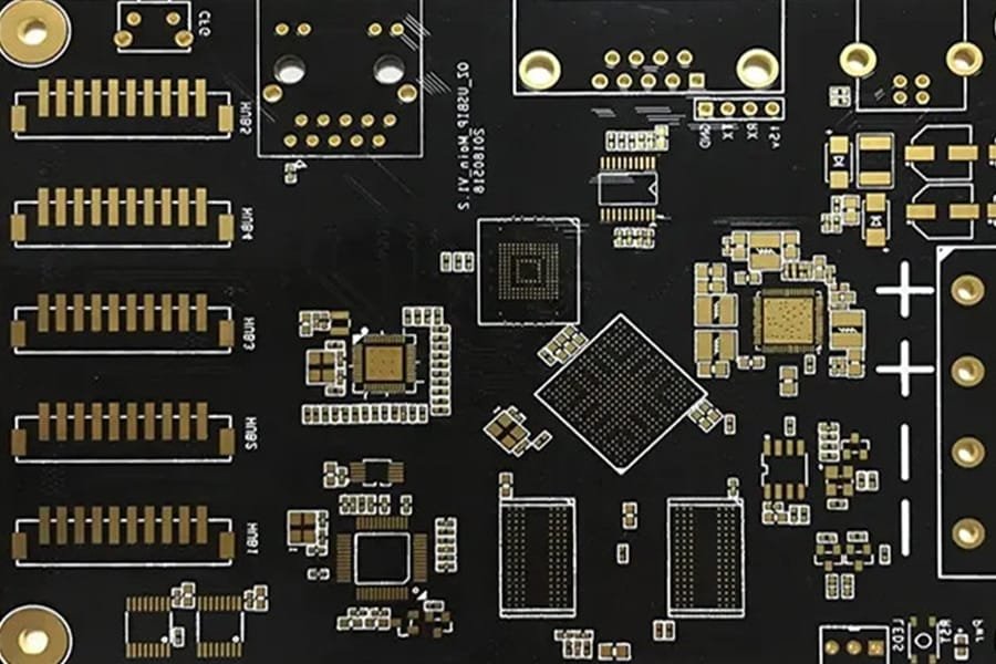
Vias enable complex functionality in printed circuit boards by facilitating vertical transitions between layers. This article provides an overview of via roles, types, reliability factors, advanced structures, and the ongoing innovation driving PCB performance.
As printed circuit boards are designed to pack more components into increasingly compact spaces, microvias play a crucial role in enabling further miniaturization. We explore the fundamentals of microvia technology and fabrication processes along with applications across consumer electronics, automotive, aerospace and medical industries.
The Essentials of Microvias – Enabling Miniaturization in PCBs Read More »
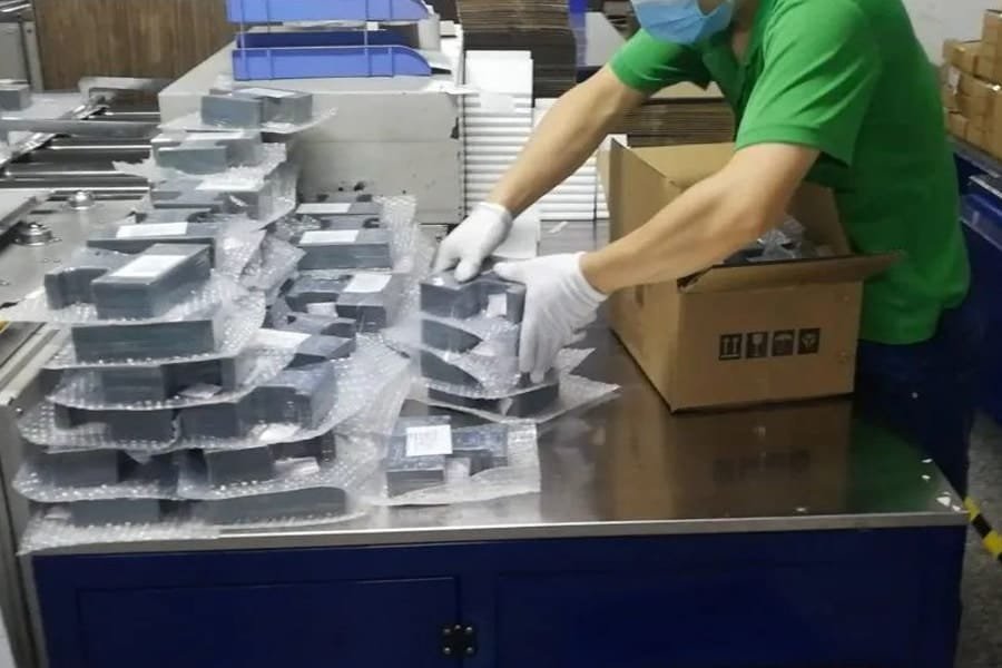
Explore the intricate journey of double-layer PCB manufacturing at JHYPCB, from routing to shipping. Witness the precision of processes like routing, V-cut, and QC, ensuring top-quality PCB fabrication.
Navigating The PCB Manufacturing Process Part 5: Testing, V-cut, QC, And Shipping Read More »

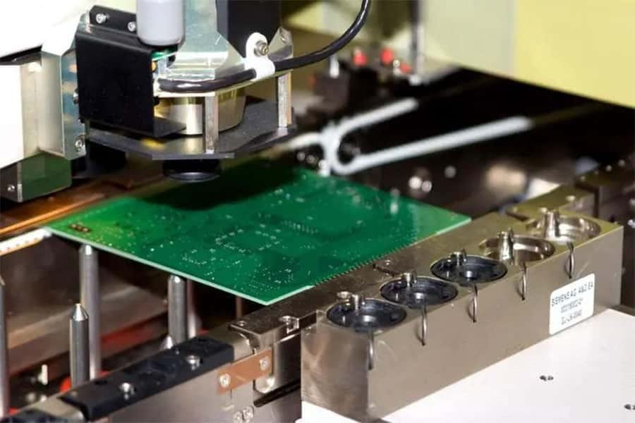
We have now covered initial PCB production processes – substrate preparation, imaging, plating, etching to form circuitry. The board is now a semi-finished product. This section explains solder mask application to shield copper traces, silkscreen printing for informational markings and labels, and surface metal treatments to protect pads from oxidation while promoting soldering. With these enhancements, boards are fully ready for electronics assembly.
Navigating The PCB Manufacturing Process Part 4: Solder Mask, Silkscreen, Surface Finish Read More »