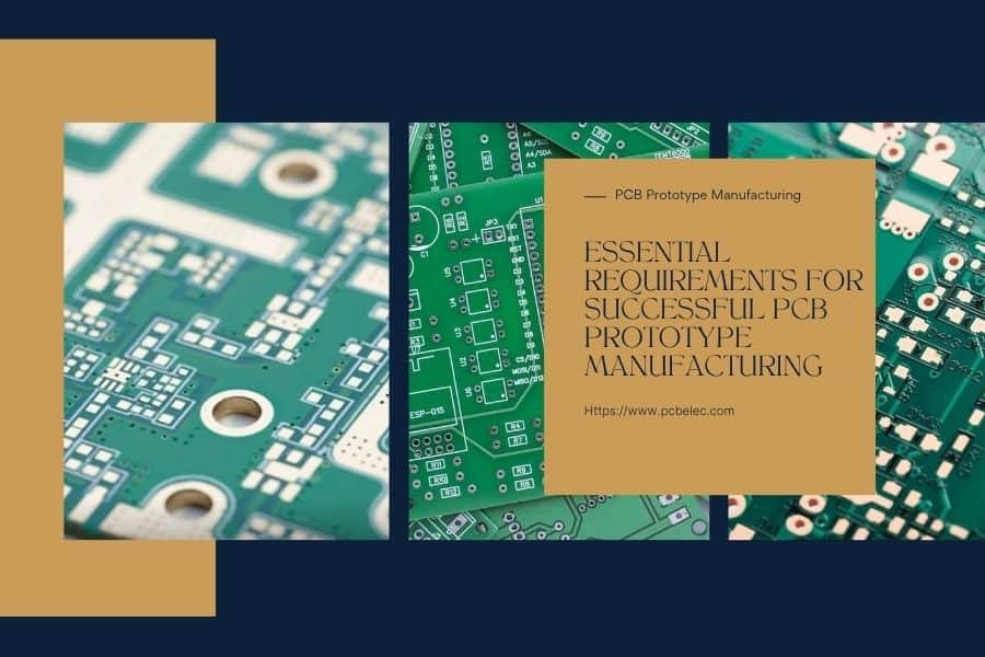
Table of Contents
PCB prototyping is a crucial step in the electronics design process, enabling designers to validate circuits and product concepts efficiently and cost-effectively. To ensure high-quality prototype boards are delivered on time, understanding the requirements for PCB prototype manufacturing is critical. By providing your PCB manufacturing partner with precise files, adhering to design rules, and supplying comprehensive documentation, you can avoid delays and errors, setting your project up for success.
This article outlines the essential requirements for PCB prototype manufacturing, from file formats to layer stackup specifications, with practical tips and industry insights to streamline your prototyping process. Whether you’re pursuing standard or quick-turn fabrication, these guidelines will help you achieve optimal results.
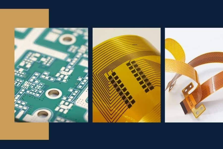
Choosing the Right Type of PCB
Selecting the appropriate PCB type is the foundation of a successful prototype. Different PCB types cater to specific applications, and understanding their characteristics ensures your design meets performance and cost requirements.
Rigid PCB
Rigid PCBs, made from solid substrates like FR-4, are the most common and cost-effective option. Their rigid structure prevents bending, making them ideal for applications such as desktop computers and industrial equipment where structural integrity is crucial. However, bending these boards can cause damage, so they’re unsuitable for compact or flexible designs.
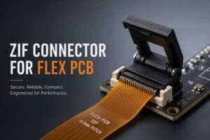
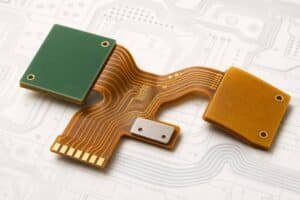
Flexible PCB
Flexible PCBs, constructed from materials like polyimide or polyester film, can bend and conform to unique shapes. They’re widely used in compact devices such as wearable electronics, cameras, and UAVs. For example, in a recent wearable fitness tracker project, our team used a flexible PCB to fit a curved housing, reducing the device’s footprint by 15%. Learn more about flexible PCB applications in our guide: Flexible PCBs: Design and Applications.
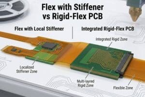
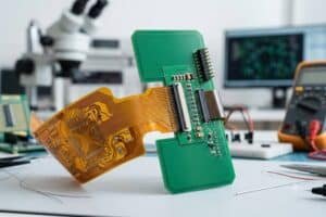
Rigid-Flex PCB
Rigid-flex PCBs combine rigid and flexible layers, offering versatility for complex designs. They’re common in aerospace and medical devices where reliability and space savings are critical. These boards balance durability with adaptability, but their manufacturing complexity increases costs.
HDI PCB
High-Density Interconnect (HDI) PCBs feature compact designs with microvias (typically <0.15 mm in diameter) and dense circuitry. They’re essential for modern devices like smartphones and 5G equipment, where high-frequency signals demand minimal transmission loss. According to a 2024 MarketsandMarkets report, the global PCB market, driven by HDI demand, is projected to reach $87.5 billion by 2028. Explore our HDI PCB Design Guidelines for best practices.
Other PCB Types
Specialty PCBs, such as LED PCBs, Aluminum PCBs, and High-TG PCBs, cater to niche applications like high-power lighting or high-temperature environments. Visit our PCB Product Catalog to explore our full range of offerings.
File Formats for PCB Prototyping
Submitting the correct file formats ensures your PCB manufacturer can accurately produce your prototype. Below are the primary formats accepted by most prototyping companies.
Gerber Files
Gerber files, an industry standard since the 1960s, are the most widely accepted format. They include separate files for copper layers, solder mask, silkscreen, and drill data. Most PCB design software (e.g., Altium, KiCad) supports Gerber exports. To avoid errors, verify your Gerber files using a viewer like Gerbv before submission.
CAD Files
Some manufacturers accept native CAD files from EDA tools like Eagle or Altium Designer, bypassing Gerber conversion. This can streamline the process but depends on the manufacturer’s supported software. Always confirm compatibility to avoid delays.
PDF Files
PDFs are suitable for simple, low-density designs but lack the precision of Gerber or CAD files. They’re prone to errors in complex prototypes, so use them sparingly.
Tip: Always include a README file with your submission to clarify file contents and design intent.
Key PCB Design Rules to Follow
Adhering to design rules ensures your PCB prototype is manufacturable and reliable. Below are critical guidelines to follow.
Trace Width and Spacing
Trace widths and clearances must meet minimum requirements to prevent shorts or overheating. For standard 1 oz copper, a minimum trace width of 0.006″ (0.15 mm) and spacing of 0.006″ are typical. Check your manufacturer’s guidelines for high-voltage or high-frequency designs.
Annular Rings
The annular ring, the bare board area around a plated through-hole, must be at least 0.004″ (0.1 mm) to ensure pad stability during soldering. Smaller rings risk pad lifting or peeling.
Via Sizes
Vias must meet minimum size requirements (typically 0.2–0.3 mm finished diameter) for reliable plating and hole filling. Microvias in HDI designs require advanced fabrication techniques, so consult your manufacturer.
Silkscreen Margins
Maintain a minimum 0.003″ (0.076 mm) clearance between silkscreen ink and copper features to prevent bleeding. Clear silkscreen enhances assembly accuracy.
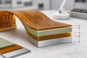
Specifying Layer Stackup Requirements
Layer stackup defines your PCB’s electrical and mechanical properties. Clear specifications are essential for accurate fabrication.
Layer Count
Specify the total number of layers (e.g., 2, 4, or 6+). Simple designs may use 2 layers, while complex circuits require more for routing flexibility. More layers increase costs, so balance performance and budget.
Materials
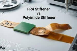
Common substrate materials include FR-4 for standard boards, polyimide for flexible PCBs, and Rogers for high-frequency applications. Specify material properties (e.g., dielectric constant) to meet performance needs.
Thickness
Define core and copper layer thicknesses. Standard FR-4 boards are 1.6 mm thick, but thinner cores (e.g., 0.8 mm) save space, while thicker cores improve heat dissipation. Copper thickness (e.g., 1 oz or 2 oz) affects current capacity.
Case Study: For a 5G antenna module, we used a 6-layer HDI PCB with a Rogers substrate and 0.8 mm thickness to optimize signal integrity and reduce size by 25%.
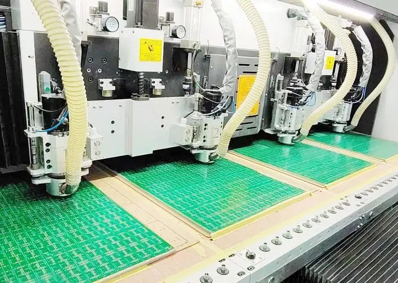
Panelization for Cost Efficiency
Panelization can reduce costs for higher-volume prototype orders but requires careful planning.
Individual Boards vs. Panelized Arrays
Individual boards suit low-volume orders, while panelized arrays are cost-effective for quantities of 10 or more. Panelization involves arranging multiple boards on a single panel, separated after fabrication.
Tooling Holes
Include 4+ precision tooling holes (typically 2–3 mm in diameter) in the panel design for accurate alignment during manufacturing.
Mouse Bites
Add V-shaped mouse bites (0.5 mm wide) between boards to facilitate separation. Specify their locations in your layout to avoid damaging traces.
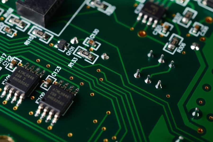
Essential Documentation for Prototyping
Comprehensive documentation ensures your PCB is manufactured and assembled correctly.
Bill of Materials (BOM)
The BOM lists all components, including part numbers, values, and quantities. A clear BOM enables accurate sourcing and assembly planning.
Assembly Drawings
Provide drawings showing layer stackup, component placement, board outline with tolerances, and special instructions. This visual guide minimizes assembly errors.
Test Procedures
Specify test parameters, methods, equipment, and pass/fail criteria for functional or electrical testing. For example, a continuity test ensures no open circuits.
Other Documentation
Include details on solder mask color, surface finish (e.g., HASL, ENIG), and packaging preferences. Clear communication prevents costly mistakes.
Understanding Lead Times
Accurate lead time planning ensures your project stays on schedule.
Standard vs. Expedited Turnaround
Standard lead times for 2–4 layer boards are typically 10–14 days, including material sourcing and fabrication. Expedited services can reduce this to 24–48 hours at a premium.
Design for Manufacturability (DFM) Check
A DFM check, taking 1–2 days, identifies layout issues before production. Address any flagged errors promptly to avoid delays.
Order Preparation
Allow 1–2 days for order processing, longer during holidays. Submit complete files and documentation to minimize administrative delays.
Common Pitfalls and How to Avoid Them
Avoid these frequent issues to ensure a smooth prototyping process:
- Incorrect Gerber Files: Use a Gerber viewer to verify layer alignment and drill data before submission.
- Inadequate Documentation: Provide a detailed BOM and assembly drawings to prevent component sourcing errors.
- Ignoring DFM Feedback: Act on DFM check results to resolve manufacturability issues early.
Tip: Partner with a manufacturer offering free DFM reviews, like [Your Company Name], to catch errors before production.
Frequently Asked Questions (FAQs)
How do I choose the right PCB type for my project?
Consider your application’s mechanical and electrical requirements. For compact designs, use flexible or HDI PCBs; for cost-sensitive projects, rigid PCBs are ideal.
What happens if my Gerber files contain errors?
Errors like misaligned layers can lead to fabrication delays. Always validate files with a Gerber viewer and request a DFM check.
Can I use PDFs for complex PCB designs?
PDFs lack the precision needed for complex designs. Stick to Gerber or CAD files for accuracy.
Conclusion
Successful PCB prototype manufacturing hinges on meeting key requirements:
- Submit Gerber or compatible CAD files for precise fabrication.
- Adhere to design rules for trace widths, vias, and silkscreen margins.
- Specify layer stackup details, including materials and thickness.
- Choose between individual or panelized boards based on order size.
- Provide a detailed BOM, assembly drawings, and test procedures.
- Plan for standard or expedited lead times, including DFM and order processing.
By partnering with an experienced PCB manufacturer like [Your Company Name], you can leverage engineering expertise to ensure flawless prototypes. Following these guidelines minimizes errors, reduces costs, and accelerates your project timeline.
Ready to Start Your PCB Prototyping Project?
Streamline your PCB prototyping process with [Your Company Name]. Our advanced fabrication techniques, including laser-drilled microvias and free DFM reviews, ensure high-quality prototypes delivered on time. Visit our PCB Prototyping Services page or contact us today to get started!