What is FPC Coverlay?
Introduction
A flexible PCB coverlay, also known as an FPC cover layer, is a critical component in flexible printed circuit boards (FPCs). This protective film, typically made of polyimide and adhesive, shields the copper circuitry of flexible PCBs from environmental damage while maintaining flexibility for bending and folding. Unlike traditional solder masks used in rigid PCBs, a flexible PCB coverlay offers superior durability and high dielectric strength, making it ideal for applications in wearables, automotive electronics, and medical devices. In this guide, we’ll explore what a flexible PCB coverlay is, its thickness, key differences from solder masks, and how it enhances FPC performance. Ready to optimize your flexible PCB design? Let’s dive in!
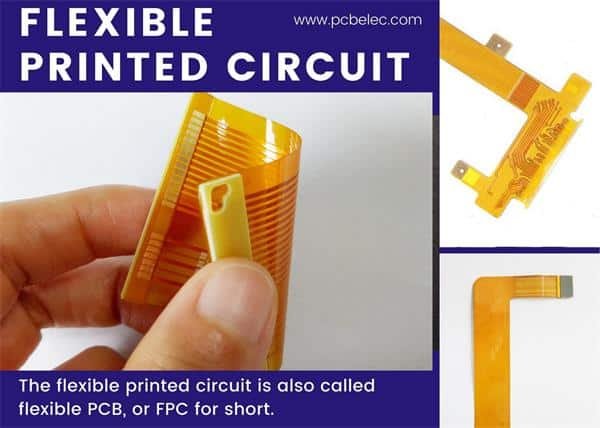
What Is a Flexible PCB?
Flexible PCBs, also known as Flexible Printed Circuits (FPCs) or Flex PCBs, are innovative circuit boards designed to bend, fold, or twist into various shapes. Unlike traditional rigid PCBs, which rely on solid substrates, flexible PCBs use lightweight, durable materials like polyimide to achieve unparalleled flexibility. This adaptability makes them a game-changer in modern electronics, from smartphones to medical implants.
Flexible PCBs save space, reduce weight, and eliminate the need for bulky connectors, making them ideal for compact devices. Their ability to conform to unique shapes supports cutting-edge applications across industries. For instance, FPCs power the folding screens in smartphones, enable compact designs in wearable fitness trackers, and enhance reliability in automotive sensors.
Key Features of Flexible PCBs
- Space and Weight Reduction: Up to 70% lighter than rigid PCBs, ideal for portable devices.
- Customizable Design: Easily tailored to fit complex shapes or tight spaces.
- Enhanced Flexibility: Supports dynamic bending for foldable electronics or solar panels.
- Improved Reliability: Reduces connection points, minimizing failure risks.
- Thermal Management: Efficient heat dissipation for high-performance circuits.
- Cost Efficiency: Lowers assembly costs by reducing connectors and simplifying installation.
Applications of Flexible PCBs
Flexible PCBs are widely used in:
- Consumer Electronics: Smartphones, tablets, and foldable displays.
- Medical Devices: Wearable monitors and implantable sensors.
- Automotive: Sensors, lighting, and infotainment systems.
- Aerospace: Satellites and lightweight avionics.
- Telecommunications: High-speed circuits with excellent signal integrity.
By enabling smaller, more reliable, and versatile electronics, flexible PCBs are at the heart of today’s technological advancements. Curious about how their protective coverlay enhances performance? Read on to learn more!
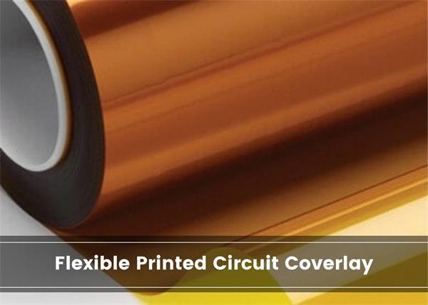
What Is Flexible PCB Coverlay?
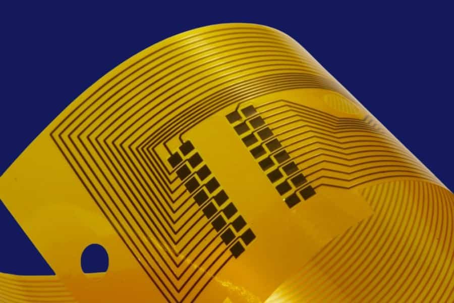
A flexible PCB coverlay, often referred to as an FPC cover layer, is a protective film that safeguards the copper circuitry of flexible printed circuit boards (FPCs). This essential component ensures durability by shielding external wiring from environmental factors like moisture, dust, and mechanical stress. Unlike traditional solder masks used in rigid PCBs, a flexible PCB coverlay is designed to maintain flexibility, making it perfect for applications requiring bending or folding, such as wearable devices and foldable smartphones.
The coverlay consists of two primary layers: a polyimide film and a flexible adhesive (typically acrylic or epoxy-based). During manufacturing, the coverlay is laminated onto the circuit under high temperature and pressure, creating a robust bond that protects the copper traces while preserving the board’s flexibility. This process ensures the FPC can withstand dynamic movements without compromising performance.
Why Use a Flexible PCB Coverlay?
- Superior Protection: Shields copper circuitry from corrosion, abrasion, and environmental damage.
- High Flexibility: Supports bending and folding, ideal for compact or dynamic applications.
- Dielectric Strength: Offers insulation with approximately 3 kV per 0.001 inch of thickness.
- Durability: Enhances the lifespan of FPCs in demanding environments like automotive or medical devices.
- Customizable: Available in various thicknesses to meet specific design needs, such as tight bending radii.
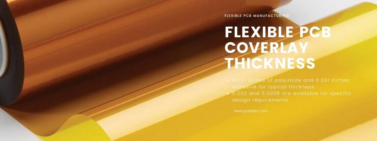
Flexible PCB Coverlay Thickness
The thickness of a flexible PCB coverlay is a critical factor in the design of flexible printed circuits (FPCs), as it directly impacts flexibility, durability, and performance. Typically, a flexible PCB coverlay consists of a polyimide film and an adhesive layer, with the most common combination being 1 mil (0.001 inches) of polyimide and 1 mil of adhesive, totaling 2 mils. However, thicknesses ranging from 0.5 mils to 2 mils are available to meet specific design requirements, such as tight bending radii or weight constraints.
Choosing the right FPC coverlay thickness depends on several factors, including the application’s bending requirements, the weight of the copper layers, and dielectric needs. For instance, thinner coverlays are ideal for highly flexible devices like foldable smartphones, while thicker coverlays provide added protection for rugged applications like automotive sensors.
Factors Influencing Coverlay Thickness
- Bending Requirements: Thinner coverlays (e.g., 0.5 mil film + 0.5 mil adhesive) support tighter bending radii, crucial for compact wearables.
- Copper Layer Weight: Heavier copper traces may require thicker coverlays for adequate protection.
- Dielectric Strength: Thicker coverlays offer higher insulation (up to 3 kV per 0.001 inch) for high-voltage applications.
- Cost Considerations: Thinner coverlays reduce material costs but may compromise durability in demanding environments.
Common Thickness Combinations
The table below outlines typical flexible PCB coverlay thickness options and their applications:
Polyimide Thickness (mil) | Adhesive Thickness (mil) | Total Thickness (mil) | Best Use Case |
|---|---|---|---|
| 1.0 | 1.0 | 2.0 | Standard FPCs (e.g., smartphones) |
| 0.5 | 0.5 | 1.0 | High-flexibility devices (e.g., wearables) |
| 2.0 | 1.0 | 3.0 | Rugged applications (e.g., automotive) |
Practical Examples
- Wearable Devices: A 1-mil total thickness coverlay ensures flexibility for smartwatch circuits while protecting against sweat and dust.
- Aerospace: A 3-mil coverlay provides robust insulation for satellite FPCs exposed to extreme temperatures.
- Medical Equipment: A 2-mil coverlay balances flexibility and durability in flexible diagnostic sensors.
Selecting the optimal coverlay thickness enhances the performance and reliability of your flexible PCB. Need help choosing the right thickness for your project? Contact our team for expert guidance!
Coverlay vs. Solder Mask: Key Differences
Both flexible PCB coverlay and solder mask serve to protect the external circuitry of printed circuit boards, but they differ significantly in composition, flexibility, and application. A flexible PCB coverlay, made of polyimide and adhesive, is tailored for flexible printed circuits (FPCs), offering superior flexibility and durability. In contrast, a solder mask, typically a liquid-based polymer, is commonly used on rigid PCBs or rigid sections of rigid-flex boards, where flexibility is less critical. Understanding these differences is essential for optimizing your PCB design.
The choice between coverlay and solder mask depends on your project’s flexibility requirements, component density, and environmental demands. For example, a coverlay is ideal for a wearable device that bends repeatedly, while a solder mask suits a rigid control board in industrial equipment.
Key Differences Between Coverlay and Solder Mask
The table below highlights the main distinctions:
Feature | Flexible PCB Coverlay | Solder Mask |
|---|---|---|
Material | Polyimide film + acrylic/epoxy adhesive | Liquid-based polymer (e.g., epoxy) |
Flexibility | High; supports dynamic bending | Limited; suitable for rigid or static applications |
Minimum Dam Size | 10 mils (prevents solder flow between pads) | 4 mils (better for fine-pitch components) |
Trace-to-Mask Opening | As close as 3 mils | Minimum 4 mils to avoid imaging issues |
Application Area | Flexible sections of FPCs or rigid-flex PCBs | Rigid PCBs or rigid sections of rigid-flex PCBs |
Fine-Pitch Compatibility | Not suitable for fine-pitch components | Ideal for high-density, fine-pitch designs |
Durability | High; resists environmental stress and flexing | Moderate; less resistant to repeated bending |
When to Use Each
- Flexible PCB Coverlay: Choose for FPCs requiring flexibility, such as in foldable smartphones, medical wearables, or automotive sensors. Its polyimide base ensures robust protection and insulation (up to 3 kV per 0.001 inch) in dynamic environments. Ensure window openings for rigid-flex designs if used across the entire board.
- Solder Mask: Opt for rigid PCBs or rigid sections of rigid-flex boards, like server motherboards or industrial controllers. Its liquid application allows precise coverage for fine-pitch components but lacks the flexibility needed for bending applications.
Applications of Flexible PCB Coverlay
Flexible PCB coverlay plays a pivotal role in enabling innovative designs across a wide range of industries by protecting flexible printed circuits (FPCs) while maintaining their ability to bend and fold. Its durability, high dielectric strength, and adaptability make it essential for compact, high-performance electronics. From consumer gadgets to critical medical equipment, the FPC coverlay ensures reliable circuit protection in dynamic applications. Below, we explore key industries where flexible PCB coverlay shines, showcasing its real-world impact.
Consumer Electronics
Flexible PCB coverlay is at the heart of modern consumer devices, enabling sleek, lightweight designs. Its flexibility supports foldable and curved circuits, making it ideal for:
- Smartphones and Tablets: Protects circuits in foldable displays, like those in next-gen foldable phones, ensuring durability despite repeated bending.
- Wearables: Shields circuitry in smartwatches and fitness trackers, allowing devices to conform to the wrist while resisting sweat and dust.
- Wireless Earbuds: Enables compact, lightweight FPCs in charging cases and earbuds, enhancing portability.
Automotive Industry
The automotive sector relies on flexible PCB coverlay for robust, space-saving electronics that withstand harsh conditions. Key applications include:
- Flexible Dashboards: Protects circuits in curved instrument panels, supporting vibrant displays and touch interfaces.
- Sensors: Insulates FPCs in tire pressure monitors or proximity sensors, ensuring reliability under vibration and temperature extremes.
- Lighting Systems: Enables flexible LED circuits for adaptive headlights, improving design flexibility and energy efficiency.
Medical Devices
In healthcare, flexible PCB coverlay ensures the reliability of life-critical electronics, particularly in compact and wearable devices. Examples include:
- Implantable Devices: Shields circuits in pacemakers or neurostimulators, offering biocompatibility and flexibility for patient comfort.
- Wearable Monitors: Protects FPCs in glucose monitors or ECG patches, ensuring consistent performance during body movement.
- Diagnostic Equipment: Supports flexible circuits in portable ultrasound devices, enabling lightweight, user-friendly designs.
Aerospace and Defense
Aerospace applications demand lightweight, durable electronics, and flexible PCB coverlay delivers. Its uses include:
- Satellites: Protects FPCs in lightweight antenna arrays, ensuring signal integrity in extreme temperatures and radiation.
- Avionics: Insulates circuits in flexible control panels, reducing weight and improving reliability in aircraft.
- Drones: Enables compact, flexible circuits for navigation and camera systems, enhancing maneuverability.
Industrial and Telecommunications
Flexible PCB coverlay supports high-speed, reliable electronics in industrial and telecom applications, such as:
- Robotics: Protects FPCs in articulated robot arms, allowing smooth movement and resistance to wear.
- 5G Infrastructure: Insulates flexible circuits in antennas and base stations, ensuring signal quality and thermal management.
- Solar Panels: Shields circuits in flexible solar arrays, enabling lightweight, portable energy solutions.
Flexible PCB Coverlay Manufacturing Process
The manufacturing process of a flexible PCB coverlay is a critical step in producing reliable flexible printed circuits (FPCs). This process involves applying a protective polyimide film and adhesive layer to shield the copper circuitry while maintaining the board’s flexibility. By carefully controlling temperature, pressure, and alignment, manufacturers ensure the FPC coverlay provides robust protection and high dielectric strength for applications like wearables, automotive sensors, and aerospace electronics. Below, we outline the key steps in the flexible PCB coverlay manufacturing process.
Step 1: Material Selection
The process begins with selecting high-quality materials tailored to the FPC’s design requirements. The coverlay typically consists of:
- Polyimide Film: A durable, flexible material (e.g., Kapton) that provides insulation and withstands high temperatures (up to 300°C).
- Adhesive Layer: Acrylic or epoxy-based adhesive ensures a strong bond between the polyimide and the circuit. Common thicknesses are 0.5–2 mils for both layers, depending on flexibility and protection needs.
Step 2: Coverlay Fabrication
The polyimide film and adhesive are pre-cut into sheets or rolls to match the FPC’s dimensions. This involves:
- Precision Cutting: Using laser or die-cutting tools to create openings for pads, vias, or components, ensuring alignment with the circuit layout.
- Surface Preparation: Cleaning the polyimide to remove contaminants, ensuring optimal adhesion during lamination.
Step 3: Alignment and Placement
The coverlay is carefully aligned with the FPC’s copper traces to ensure accurate coverage. This step is critical to avoid misalignment, which could expose circuitry or compromise functionality. Automated alignment systems or fiducial markers are often used for precision, especially in high-density designs like those in smartphones or medical devices.
Step 4: Lamination
The coverlay is bonded to the FPC through a lamination process, which involves:
- Heat Application: Temperatures typically range from 150–200°C to activate the adhesive and bond the polyimide to the circuit.
- Pressure Control: Uniform pressure (e.g., 100–300 psi) ensures a secure, bubble-free bond without damaging delicate copper traces.
- Vacuum Lamination: Often used to eliminate air pockets, enhancing adhesion and durability, especially for aerospace or medical applications.
Step 5: Curing and Inspection
After lamination, the FPC undergoes:
- Curing: A controlled cooling process to solidify the adhesive bond, ensuring long-term stability.
- Quality Inspection: Automated optical inspection (AOI) or manual checks verify alignment, adhesion, and coverage. Tests confirm dielectric strength (approximately 3 kV per 0.001 inch) and flexibility.
Step 6: Final Processing
The FPC may undergo additional steps, such as:
- Trimming: Removing excess coverlay material for a clean finish.
- Testing: Flexing tests ensure the coverlay withstands bending without cracking, critical for applications like foldable displays or wearable sensors.
Benefits and Limitations of Flexible PCB Coverlay
Flexible PCB coverlay is a cornerstone of flexible printed circuit (FPC) design, offering unique advantages for protecting circuits in dynamic applications. However, like any technology, it has limitations that designers must consider to ensure optimal performance. Understanding the benefits and drawbacks of FPC coverlay helps you make informed decisions for projects in industries like wearables, automotive, and aerospace. Below, we explore the key advantages and limitations, along with strategies to maximize its effectiveness.
Benefits of Flexible PCB Coverlay
Flexible PCB coverlay provides several critical advantages that make it ideal for modern electronics:
- Superior Flexibility: Supports repeated bending and folding, perfect for applications like foldable smartphones or wearable health monitors.
- Robust Protection: Shields copper circuitry from moisture, dust, chemicals, and mechanical stress, enhancing durability in harsh environments like automotive sensors.
- High Dielectric Strength: Offers insulation up to 3 kV per 0.001 inch, ensuring safety in high-voltage applications such as medical implants.
- Customizable Thickness: Available in various thicknesses (0.5–2 mils polyimide + adhesive), allowing tailored solutions for specific bending or weight requirements.
- Enhanced Reliability: Reduces risks of circuit exposure or damage, improving the lifespan of FPCs in dynamic settings like aerospace avionics.
Limitations of Flexible PCB Coverlay
Despite its strengths, flexible PCB coverlay has some constraints:
- Higher Cost: Polyimide and adhesive materials are more expensive than liquid solder masks, increasing production costs for budget-sensitive projects.
- Limited Fine-Pitch Compatibility: Not suitable for high-density, fine-pitch components due to larger dam sizes (minimum 10 mils), unlike solder masks (4 mils).
- Complex Application Process: Requires precise alignment and lamination, which can increase manufacturing time and complexity compared to solder mask application.
- Thickness Trade-Offs: Thinner coverlays enhance flexibility but may reduce durability, while thicker options add weight, impacting compact designs.
- Not Ideal for Rigid Sections: Less effective on rigid PCB sections, where solder masks are preferred unless window openings are used in rigid-flex designs.
Pros and Cons Comparison
The table below summarizes the benefits and limitations of flexible PCB coverlay:
| Aspect | Pros | Cons |
|---|---|---|
| Flexibility | Supports dynamic bending for foldable devices | May require thinner layers, reducing durability |
| Protection | Shields against environmental stress | Higher material costs than solder masks |
| Dielectric Strength | High insulation (3 kV per 0.001 inch) | Limited suitability for fine-pitch components |
| Application | Customizable for various design needs | Complex lamination process increases production time |
| Versatility | Ideal for flexible and rigid-flex PCBs | Less effective on fully rigid PCB sections |
Mitigating Limitations
To address the limitations of flexible PCB coverlay:
- Hybrid Designs: Combine coverlay on flexible sections with solder mask on rigid areas for cost-effective rigid-flex PCBs.
- Cost Optimization: Use thinner coverlays for less demanding applications to reduce material costs while maintaining flexibility.
- Partner with Experts: Work with experienced manufacturers to streamline the lamination process and ensure precise alignment, minimizing production challenges.
- Prototype Testing: Test coverlay thickness and performance early in the design phase to balance flexibility and durability, especially for wearables or automotive applications.
Choosing the Right Flexible PCB Coverlay for Your Project
Selecting the optimal flexible PCB coverlay is crucial for ensuring the performance, durability, and cost-effectiveness of your flexible printed circuit (FPC) design. The right coverlay balances flexibility, protection, and application-specific requirements, such as bending radius or environmental resistance. Whether you’re designing wearables, automotive sensors, or aerospace components, this guide will help you make an informed choice.
Key Considerations for Choosing a Flexible PCB Coverlay
Use this checklist to select the best FPC coverlay for your project:
- Bending Requirements: Determine the minimum bending radius. Thinner coverlays (e.g., 0.5 mil polyimide + 0.5 mil adhesive) are ideal for tight bends in devices like foldable smartphones.
- Environmental Conditions: Assess exposure to moisture, heat, or chemicals. A thicker coverlay (e.g., 2 mil polyimide + 1 mil adhesive) offers enhanced protection for rugged applications like automotive electronics.
- Dielectric Needs: Ensure sufficient insulation for high-voltage applications. Polyimide coverlays provide approximately 3 kV per 0.001 inch of thickness.
- Copper Layer Weight: Heavier copper traces may require a thicker coverlay to ensure adequate coverage and protection.
- Budget Constraints: Thinner coverlays reduce material costs but may compromise durability. Balance cost with performance needs.
- Application Type: Consider the end use. For example, medical devices require biocompatible coverlays, while aerospace applications prioritize lightweight materials.
Practical Tips for Coverlay Selection
- Consult with Manufacturers Early: Work with your PCB supplier to match coverlay specifications to your design goals. They can recommend thickness combinations based on your prototype.
- Test for Flexibility: Request samples to evaluate bending performance, especially for dynamic applications like wearable fitness trackers.
- Consider Hybrid Designs: For rigid-flex PCBs, combine coverlay on flexible sections with solder mask on rigid areas for optimal performance.
- Prioritize Quality: Choose high-grade polyimide coverlays to ensure long-term reliability, especially in high-stress environments like aerospace or medical devices.
Example Decision Process
For a smartwatch, select a 1-mil total thickness coverlay (0.5 mil polyimide + 0.5 mil adhesive) to support frequent bending while protecting circuits from sweat. For an automotive sensor, opt for a 3-mil coverlay (2 mil polyimide + 1 mil adhesive) to withstand heat and vibration.
FAQ About Flexible PCB Coverlay
Have questions about flexible PCB coverlay? We’ve compiled answers to common queries to help you understand its role in flexible printed circuit (FPC) design and how it can enhance your projects.
What is the purpose of a flexible PCB coverlay?
A flexible PCB coverlay protects the copper circuitry of FPCs from environmental factors like moisture, dust, and mechanical stress. It provides insulation, supports bending, and ensures durability in applications like wearables, automotive sensors, and medical devices.
How does a flexible PCB coverlay differ from a solder mask?
Unlike a solder mask, which is a liquid-based polymer used on rigid PCBs, a flexible PCB coverlay is a polyimide film with adhesive, offering greater flexibility and durability. Coverlays are ideal for dynamic applications, while solder masks suit rigid or fine-pitch designs.
What is the typical thickness of an FPC coverlay?
The standard thickness is 1 mil polyimide and 1 mil adhesive (2 mils total). Thinner options (e.g., 0.5 mil + 0.5 mil) are used for high-flexibility needs, while thicker coverlays (e.g., 2 mil + 1 mil) suit rugged applications.
Can a flexible PCB coverlay be used on rigid-flex PCBs?
Yes, coverlays are commonly used on the flexible sections of rigid-flex PCBs. For rigid sections, a solder mask is typically applied, but coverlays can cover the entire board if window openings are included.
Start Your Flexible PCB Project Today
Ready to harness the power of flexible PCB coverlay for your next project? Whether you’re designing cutting-edge wearables, automotive sensors, or aerospace components, a well-chosen FPC coverlay ensures durability, flexibility, and top-notch circuit protection. Our team at PCB Elec specializes in crafting high-quality flexible printed circuits tailored to your unique needs.
Don’t let complex design requirements hold you back. Explore our flexible PCB solutions, from selecting the ideal coverlay thickness to optimizing for high-performance applications. Contact us now for a free consultation or request a quote to kickstart your flexible circuit design!
Related Reading
- A Complete Guide To Single-Sided Flex Circuits
- A Completed Guide Of Double-Sided Flexible PCB
- Everything You Need To Know About Multilayer Flexible PCB
- What is Flexible PCB Prototype?
- What Are Flexible PCB Stiffeners?
- Rigid PCB vs Flex PCB: What Is The Difference?
- The Manufacturing Process Of Double-sided Flexible PCB Coverlay
- Custom Flex PCB:Tailored Solutions for Your Applications
- Finding the Right China PCB Manufacturers:5 Vetting Tips
- Introduction to Semi-Flex PCBs: Bridging Rigid and Flex PCBs
- Flexible PCB Manufacturing: A Guide to Fabrication and Assembly
- Flexible PCB MaHow to Select the Right Flexible PCB Manufacturer for Your Product: A 6-Step Guidenufacturing: A Guide to Fabrication and Assembly
- What Are The Types of Flexible Circuit Boards?
- Top Applications of Flexible Printed Circuit Boards in 2024
- What Are The Advantages And Applications Of Rigid-Flex PCBs?