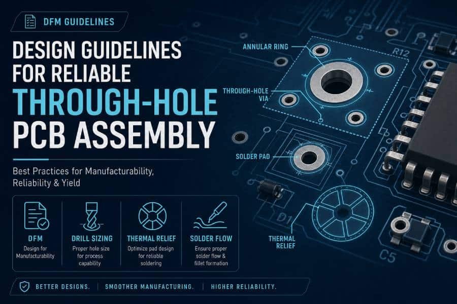
PCB Design

high frequency pcbs for 5g base stations and small cells design & manufacturing tips

High Frequency PCBs for 5G Base Stations and Small Cells | Design & Manufacturing Tips

High frequency PCBs are at the core of 5G macro base stations and small cells, where Sub‑6 and mmWave signals demand low loss, tight impedance control, and robust reliability in harsh outdoor environments. This guide shares practical design and manufacturing tips—from material and stackup choices to RF layout, thermal, and DFM checks—to help you turn 5G concepts into stable, high‑volume hardware.

High Frequency PCBs for 5G Base Stations and Small Cells | Design & Manufacturing Tips Read More »

Hybrid High Frequency PCBs: Combining Rogers and FR4 for RF and Digital Integration

Hybrid High Frequency PCBs: Combining Rogers and FR4 for RF and Digital Integration

Hybrid high frequency PCBs use Rogers for critical RF layers and FR4 for digital, control, and power layers in a single stackup. This article explains why and when to choose a hybrid design, shows common Rogers+FR4 stackup patterns, and shares practical layout and manufacturing guidelines so your RF and digital sections work together without blowing up the budget.

Hybrid High Frequency PCBs: Combining Rogers and FR4 for RF and Digital Integration Read More »

High Frequency PCB Design Guidelines: Layout, Stackup and Impedance Control

High Frequency PCB Design Guidelines: Layout, Stackup and Impedance Control

High frequency PCB design requires much stricter rules than low‑speed layouts. This guide explains practical high frequency PCB design guidelines for stackup planning, controlled impedance, routing, grounding and crosstalk control, so your RF and high‑speed boards can be manufactured reliably with stable signal integrity.

High Frequency PCB Design Guidelines: Layout, Stackup and Impedance Control Read More »

3D view of a green PCB with bright gold finger edge connector in the foreground and a blurred Gerber layout in the background, illustrating a DFM checklist review before sending gold finger PCB Gerber files.

Gold Finger PCB DFM Checklist: 10 Things to Check Before Sending Gerbers

Gold finger PCBs fail in the field more often because of DFM oversights than connector theory. This checklist walks you through 10 things to verify before sending Gerber files, from finger geometry, bevel and finish definitions to copper clearances, keep-outs, and panelization. Use it as a last pre-flight check to catch issues early and make your manufacturer’s DFM review much smoother.

Gold Finger PCB DFM Checklist: 10 Things to Check Before Sending Gerbers Read More »

how to panelize and route gold finger pcbs for better yield and reliability

How to Panelize and Route Gold Finger PCBs for Better Yield and Reliability

Panelization and routing choices can make or break the yield and reliability of gold finger PCBs. This practical guide shows how to orient boards on the panel, place routing and break‑off tabs around the connector edge, use fiducials and keep‑outs, and route high‑speed and power signals into edge fingers without compromising manufacturability.

How to Panelize and Route Gold Finger PCBs for Better Yield and Reliability Read More »

Blog cover showing a PCB edge connector with bright gold fingers split between hard gold and ENIG themed colors, illustrating a comparison of finishes for PCB gold fingers.

Hard Gold vs ENIG for PCB Gold Fingers: Which Finish Should You Choose?

Hard gold and ENIG are the two most common finishes used on PCB gold fingers, but they behave very differently in real applications. This article explains how each finish is applied, compares wear resistance, solderability, corrosion performance and cost, and then walks through practical recommendations so you can decide whether your edge connectors really need hard gold or if ENIG is good enough.

Hard Gold vs ENIG for PCB Gold Fingers: Which Finish Should You Choose? Read More »

gold finger pcb design rules

Gold Finger PCB Design Rules: Avoiding Common Pitfalls for Reliable Connections

Gold finger PCBs are the backbone of many plug‑in cards and edge‑connector boards, but small design mistakes can quickly lead to contact failures and production issues. This article walks through the key gold finger PCB design rules, shows the most common layout pitfalls with practical tips to fix them, and explains what information your fabricator needs for a reliable gold finger PCB fabrication service.

Gold Finger PCB Design Rules: Avoiding Common Pitfalls for Reliable Connections Read More »

Blog cover illustrating a choice between a standard low-speed PCB and a high-speed PCB with highlighted controlled-impedance differential pairs.

Do You Really Need Controlled Impedance for Your PCB Design?

Wondering if your next board really needs controlled impedance or if standard fabrication is enough? This article walks through the key factors that drive the decision – signal speed, trace length, interface standards, product criticality and cost – and outlines practical cases where controlled impedance is essential, where it is optional and how to choose the right level of impedance control together with your PCB manufacturer.

Do You Really Need Controlled Impedance for Your PCB Design? Read More »

Scroll to Top