
PCB Design

how to panelize and route gold finger pcbs for better yield and reliability

How to Panelize and Route Gold Finger PCBs for Better Yield and Reliability

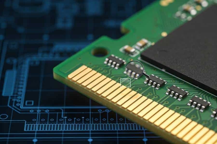
Panelization and routing choices can make or break the yield and reliability of gold finger PCBs. This practical guide shows how to orient boards on the panel, place routing and break‑off tabs around the connector edge, use fiducials and keep‑outs, and route high‑speed and power signals into edge fingers without compromising manufacturability.

How to Panelize and Route Gold Finger PCBs for Better Yield and Reliability Read More »

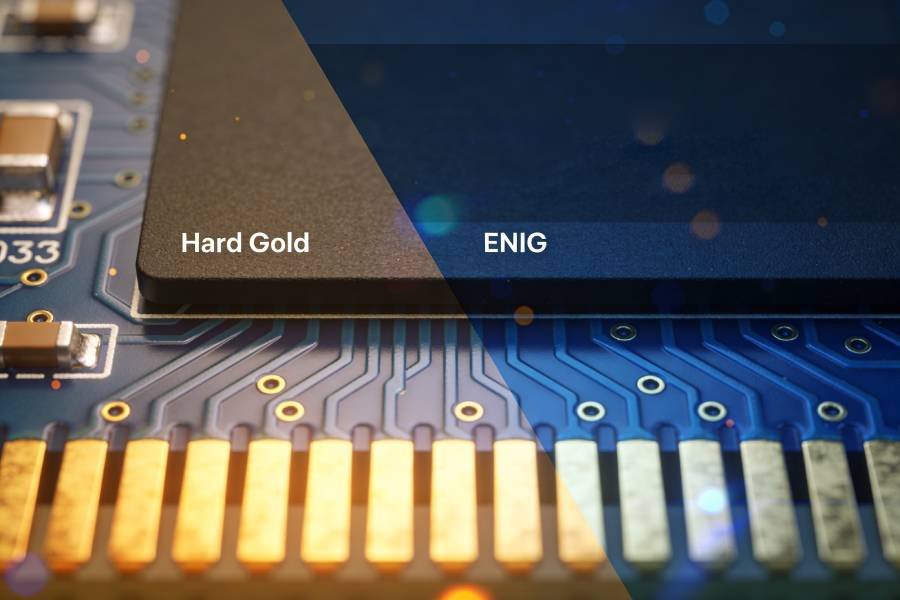
Blog cover showing a PCB edge connector with bright gold fingers split between hard gold and ENIG themed colors, illustrating a comparison of finishes for PCB gold fingers.

Hard Gold vs ENIG for PCB Gold Fingers: Which Finish Should You Choose?

Hard gold and ENIG are the two most common finishes used on PCB gold fingers, but they behave very differently in real applications. This article explains how each finish is applied, compares wear resistance, solderability, corrosion performance and cost, and then walks through practical recommendations so you can decide whether your edge connectors really need hard gold or if ENIG is good enough.

Hard Gold vs ENIG for PCB Gold Fingers: Which Finish Should You Choose? Read More »

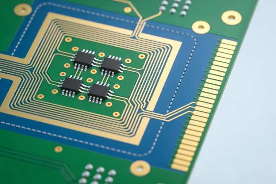
gold finger pcb design rules

Gold Finger PCB Design Rules: Avoiding Common Pitfalls for Reliable Connections

Gold finger PCBs are the backbone of many plug‑in cards and edge‑connector boards, but small design mistakes can quickly lead to contact failures and production issues. This article walks through the key gold finger PCB design rules, shows the most common layout pitfalls with practical tips to fix them, and explains what information your fabricator needs for a reliable gold finger PCB fabrication service.

Gold Finger PCB Design Rules: Avoiding Common Pitfalls for Reliable Connections Read More »

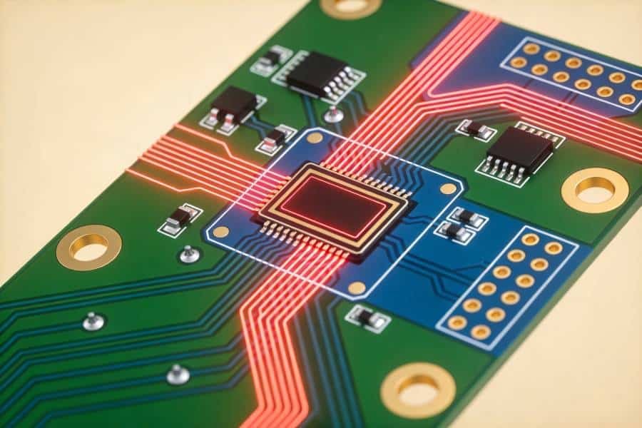
Blog cover illustrating a choice between a standard low-speed PCB and a high-speed PCB with highlighted controlled-impedance differential pairs.

Do You Really Need Controlled Impedance for Your PCB Design?

Wondering if your next board really needs controlled impedance or if standard fabrication is enough? This article walks through the key factors that drive the decision – signal speed, trace length, interface standards, product criticality and cost – and outlines practical cases where controlled impedance is essential, where it is optional and how to choose the right level of impedance control together with your PCB manufacturer.

Do You Really Need Controlled Impedance for Your PCB Design? Read More »

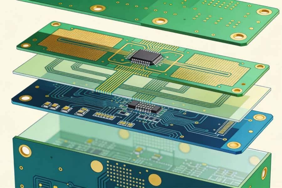
Blog cover showing a multilayer PCB stackup and controlled impedance traces for a high-speed stackup design guide.

PCB Impedance Control Stackup Design Guide for High‑Speed Signals

A good stackup is the foundation of any impedance‑controlled PCB. This guide explains the key parameters that shape trace impedance, compares common microstrip and stripline structures, walks through example stackups for high‑speed designs and shows how to collaborate with your PCB manufacturer to turn your impedance targets into a manufacturable, reliable board.

PCB Impedance Control Stackup Design Guide for High‑Speed Signals Read More »

single sided flexible pcb design

Single-Sided Flexible PCB Design Guide: Bending Radius, Trace Routing and Stiffeners

Single-sided flexible PCBs look simple, but poor design on bending radius, trace layout or stiffener placement can quickly lead to cracks and failures. This design guide walks you through practical rules for setting minimum bend radius, routing traces in flex areas and using stiffeners correctly, so your single-sided flex circuits stay reliable in both static and dynamic applications.

Single-Sided Flexible PCB Design Guide: Bending Radius, Trace Routing and Stiffeners Read More »

led pcb thermal management

Thermal Management in LED PCB: How to Prevent Overheating (2026 Engineering Guide)

LED junction temperatures above 85°C cut lifespan by 50%+. This deep dive covers aluminum LED PCB thermal engineering: MCPCB dielectric k-values (1-8 W/m·K), thermal via arrays (8-12/cm²), copper thickness optimization (2-3oz), heatsink TIM interfaces, FEA simulation workflows, and JEDEC51 validation testing. Essential strategies for street lights, automotive and industrial LED designs ensuring L70>50,000 hours reliability.

Thermal Management in LED PCB: How to Prevent Overheating (2026 Engineering Guide) Read More »

led pcb design guide

LED PCB Design Guide: Best Practices for Optimal Performance

Designing LED PCBs demands far more than applying standard PCB design rules. While conventional circuit boards prioritize electrical performance and signal integrity, LED PCBs must engineer thermal pathways as meticulously as electrical circuits—because heat, not electrons, determines whether your LED product succeeds or fails. A single design oversight—insufficient copper pour, poorly placed thermal vias, or inadequate LED spacing—can transform a promising LED design into a field failure nightmare. This comprehensive 2026 guide walks you through every critical aspect of LED PCB design, from substrate selection and power calculations through advanced thermal simulation and design for manufacturing. Whether you’re designing your first LED circuit or optimizing an existing product, you’ll discover proven techniques for maximizing LED lifespan, ensuring uniform light output, and avoiding the costly mistakes that plague poorly designed LED PCBs. Learn how proper thermal via placement can reduce junction temperatures by 20-30°C, why 2oz copper outperforms 1oz despite minimal cost increase, and when thermal simulation transitions from optional to mandatory.

LED PCB Design Guide: Best Practices for Optimal Performance Read More »

Scroll to Top