Table of Contents
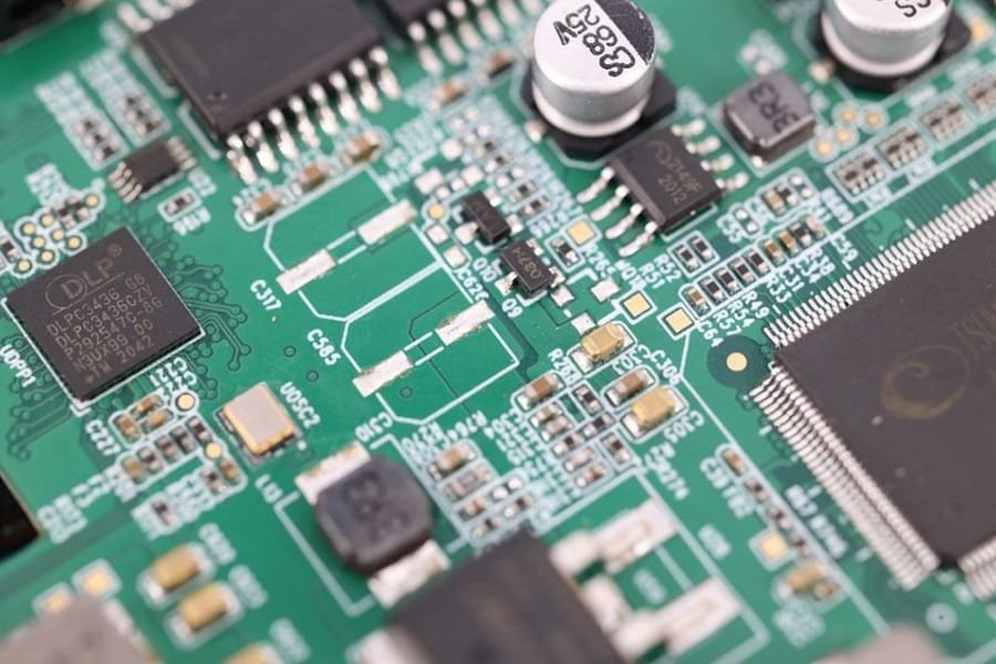
As electronic devices trend toward miniaturization and high-density designs, Surface Mount Technology (SMT) dominates the PCB assembly process, while through-hole components remain vital for specialized applications. This results in mixed technology PCB assembly (combining SMT and through-hole) or full surface-mount assembly. At JHYPCB, we leverage advanced equipment and IPC-A-610 standards to deliver reliable PCBA solutions for industries like 5G, medical, and automotive. This comprehensive guide details the PCB assembly process, provides a flow chart, and shares expert insights to optimize your project.
PCB Assembly Process: A Step-by-Step Breakdown
Step 1: Component Procurement and Design for Manufacturability (DFM)
The PCB assembly process starts with procuring components based on the client’s Bill of Materials (BOM). If components are unavailable, JHYPCB collaborates with clients to source IPC-compliant alternatives, ensuring performance and compatibility.
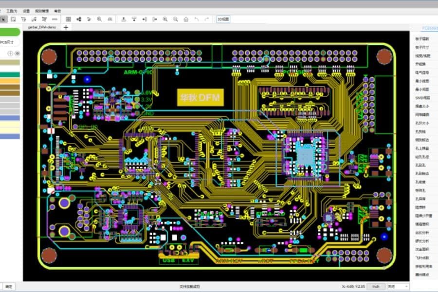
Design for Manufacturability (DFM) is critical to avoid costly errors. Our engineers analyze Gerber files, BOM, and schematics to optimize component placement, trace routing, and solderability. For example, ensuring 0.1 mm clearance between fine-pitch components prevents bridging during soldering.
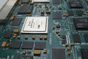
Step 2: PCB Fabrication
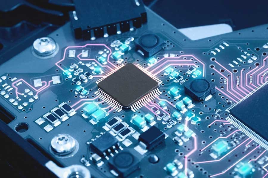
The bare PCB is fabricated using client specifications, creating the substrate, copper traces, vias, and solder mask. For high-density interconnect (HDI) boards, microvias and sequential lamination ensure compact, high-performance designs.
Step 3: Solder Paste Application
Solder paste, a blend of solder particles and flux, is applied to PCB pads using a stainless steel stencil. A stencil printer deposits paste precisely where components will be placed, preventing defects like solder bridges. For HDI boards, stencil thickness (typically 0.1–0.15 mm) is critical for fine-pitch components.
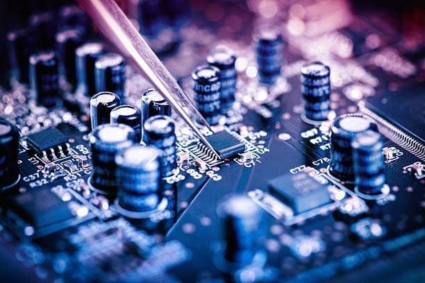
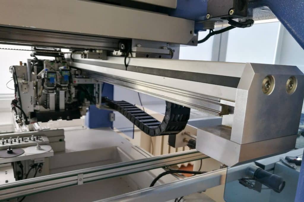
Step 4: Pick and Place
Automated Pick and Place machines use vacuum nozzles to place components with ±0.01 mm accuracy, guided by design files. Component reels are loaded into the machine, ensuring speed and precision for high-volume production. For mixed assemblies, through-hole components are manually or semi-automatically placed.
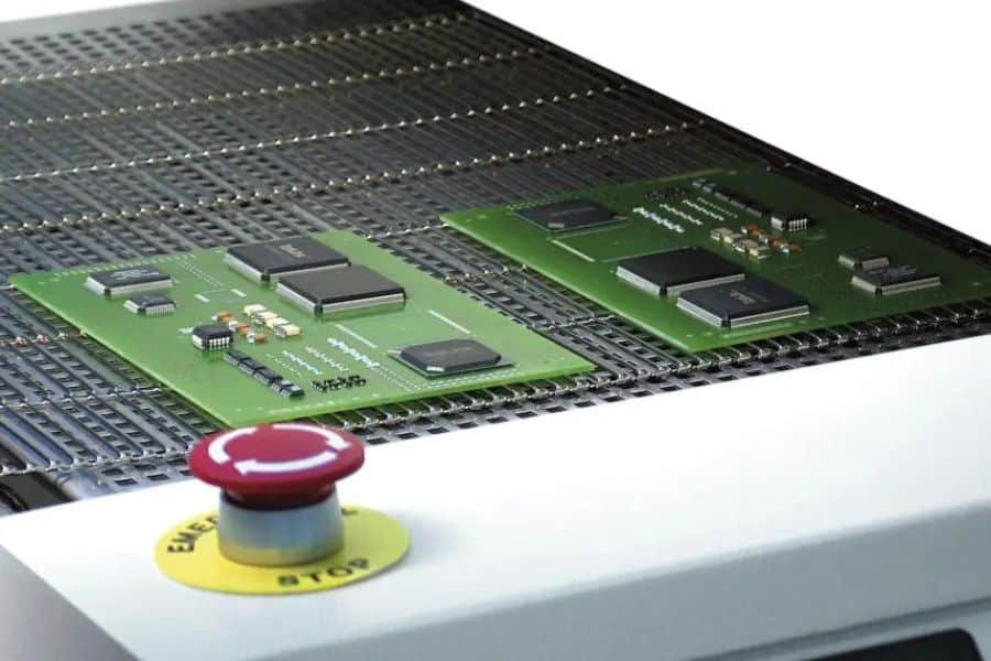
Step 5: Reflow Soldering
In reflow soldering, the PCB passes through a reflow oven on a conveyor belt. A controlled temperature profile—150°C preheat, 180–200°C soak, and 240–260°C peak for lead-free solder (e.g., SAC305)—melts the paste, forming robust connections. For HDI boards, tighter profiles prevent thermal shock to fine-pitch components.
Key Parameters for Optimal Reflow
- Temperature Profile: Balanced ramp-up and cooling prevent defects like tombstoning or voids.
- Solder Paste Type: Lead-free solder ensures RoHS compliance but requires higher temperatures.
- Oven Calibration: Real-time monitoring minimizes defects, achieving 99% consistency.
Common Reflow Challenges
- Tombstoning: Uneven heating lifts small components, mitigated by balanced profiles.
- Solder Voids: Gas entrapment weakens joints, reduced by vacuum reflow or optimized paste volume.
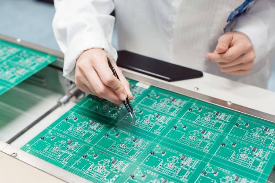
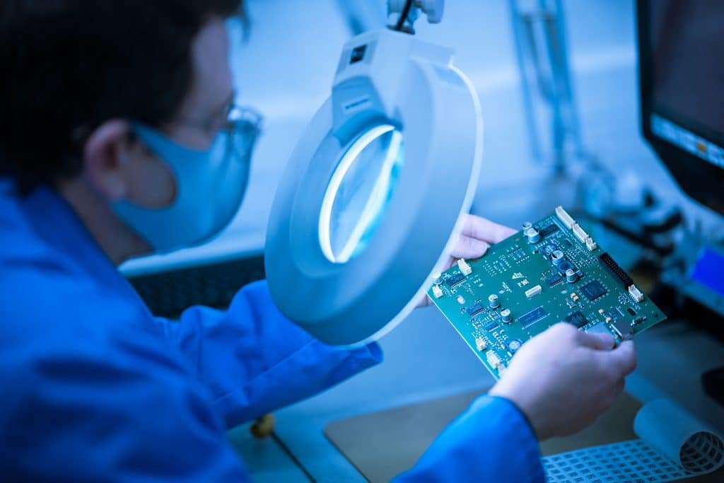
Step 6: Inspection
Inspection ensures quality by detecting defects like short circuits, misalignments, or poor solder joints. JHYPCB uses a multi-tiered approach:
Manual Inspection
Technicians visually check for obvious issues, such as excess solder or component misalignment, as a quick first step.
Automated Optical Inspection (AOI)
AOI uses high-resolution cameras to analyze PCBs from multiple angles, detecting surface-level defects like missing components or solder bridges. It’s ideal for high-volume production, processing 500 boards per hour.
X-ray Inspection
X-ray inspection reveals hidden joints in multilayer or HDI PCBs. By analyzing reflected X-rays, technicians identify voids, misalignments, or incomplete joints with 99.5% accuracy, critical for high-density designs.
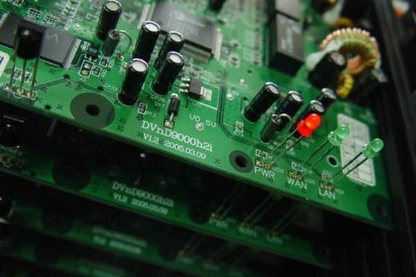
Step 7: Final Testing
Final testing verifies functionality using In-Circuit Testing (ICT), Functional Testing, or Boundary Scan. For example, ICT checks electrical continuity, while functional testing simulates real-world conditions. Once validated, the PCBA is packaged and shipped.

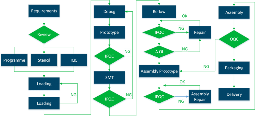
Electronic PCB Assembly Process Flow Chart
The flow chart below visualizes the PCB assembly process, from procurement to testing.
Industry Applications of PCB Assembly
PCB assembly varies by industry, each with unique requirements:
- 5G Telecommunications: High-frequency PCBs demand materials like Rogers substrates for impedance control.
- Medical Devices: Biocompatible materials and stringent testing ensure reliability for pacemakers or imaging systems.
- Automotive: HDI boards with thermal management support advanced driver-assistance systems (ADAS).
- Consumer Electronics: Flexible PCBs enable compact designs for wearables and smartphones.
2025 Trends in PCB Assembly
- AI in Inspection: AI-driven AOI and X-ray systems improve defect detection by 30%, reducing costs and time.
- Eco-Friendly Assembly: RoHS-compliant, lead-free processes and recyclable materials align with global regulations.
- Industry 4.0: IoT-enabled equipment monitors reflow ovens in real-time, boosting efficiency by 20%.
- Miniaturization: HDI and flexible PCBs support 5G and IoT devices, requiring advanced assembly techniques.
Industry Forecast: A 2025 MarketsandMarkets report predicts the global PCB market will reach $92.4 billion by 2030, with a 5.7% CAGR, driven by 5G and IoT demand.
FAQ: Your PCB Assembly Questions Answered
What are the most common PCB assembly defects?
Defects like solder bridges, tombstoning, and voids arise from improper paste application or reflow settings. JHYPCB’s advanced processes minimize these issues.
How can I reduce PCB assembly costs?
Optimize your BOM, use standard components, and conduct a DFM review. JHYPCB’s free DFM Consultation can save up to 20% on costs.
What’s the difference between wave soldering and reflow soldering?
Wave soldering suits through-hole components, using a molten solder wave, while reflow soldering is ideal for SMT, relying on controlled heat.
How does PCB assembly differ for HDI boards?
HDI boards require laser-drilled microvias, precise solder paste application, and advanced inspection due to their compact designs.
What role does AI play in PCB assembly?
AI enhances inspection by analyzing AOI and X-ray images with 99% accuracy, reducing human error and speeding up quality control.
Why JHYPCB for Your PCB Assembly Needs?
JHYPCB combines cutting-edge technology, IPC-A-610 compliance, and 20+ years of expertise to deliver high-quality PCBA solutions. Our clients in 5G, medical, and automotive industries trust us for precision and reliability. Start your project today with our Free Quote or download our DFM Checklist.
Related Posts
- How to Select the Right Low-volume PCB Assembly Manufacturer?
- The Advantages and Disadvantages of Surface Mount Technology (SMT)
- How to clean the PCB assembled boards? [Solved]
- Selective Wave Soldering Guidelines
- SMT PCB Assembly Manufacturing Process Introduces
- The Two Typical SMT Reflow Soldering Temperature Curve Modes
- 30 Common SMT PCB Assembly Defects
- Solder Paste and Solder Paste Printing in SMT PCB Assembly
- IPC Standards: A Guide to Standards for PCB Manufacturing and Assembly
- What is the Bill of Materials(BOM) and how to create one?
- One-Stop Solution: The Advantages of Turnkey PCB Manufacturing and Assembly