
Table of Contents
Multilayer PCBs are the backbone of modern electronics, enabling compact, high-performance devices in industries like telecommunications, medical, and automotive. This guide explores the essentials of multilayer PCB stack-up, manufacturing processes, quality standards, and storage tips to help you design and produce reliable PCBs. Whether you’re a beginner or an experienced engineer, this article provides actionable insights to optimize your multilayer PCB projects.

What is a Multilayer PCB?
A multilayer PCB consists of multiple layers of conductive copper and insulating materials stacked together, typically ranging from 4 to over 50 layers for complex applications. Unlike single- or double-layer PCBs, multilayer designs offer higher circuit density, improved signal integrity, and efficient power distribution, making them ideal for advanced electronics like smartphones, servers, and avionics systems.
Key Terms Explained
- Core: A rigid substrate (e.g., FR-4) with copper foil on both sides, forming the inner layers of a PCB.
- Prepreg: Uncured epoxy resin-impregnated glass cloth used to insulate and bond layers during lamination.
- Surface Layers: The top and bottom layers where components are mounted, critical for signal routing and connectivity.
Understanding Multilayer PCB Stack-Up
The stack-up defines how layers are arranged in a multilayer PCB, impacting performance factors like signal integrity, thermal management, and electromagnetic interference (EMI). Symmetry is preferred, so even-numbered layers (e.g., 4, 6, 8) are more common than odd-numbered ones, as they provide better mechanical strength.
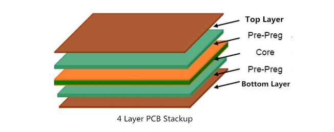
4-Layer PCB Stack-Up and Thickness
A 4-layer PCB is the simplest multilayer configuration, consisting of one core (two inner layers) and two surface layers. The core, typically 0.014″ thick with 1 oz copper, is sandwiched between prepreg layers for insulation. Surface layers, often 0.5 oz copper with plating, host components. The total thickness is usually 1.6 ± 0.16 mm.
Example Application: A 4-layer PCB is ideal for consumer electronics, such as smart home devices, balancing cost and performance.


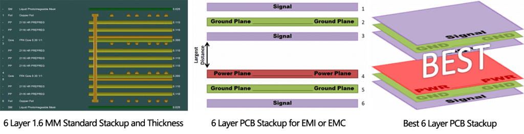
6-Layer PCB Stack-Up and Thickness
A 6-layer PCB adds another core, resulting in four inner layers and two surface layers. This setup supports moderate complexity, such as industrial control systems or automotive sensors. The stack-up includes two cores (each with two conductive layers) separated by prepreg, with a typical thickness of 1.6–2.0 mm.
Design Tip: Dedicate inner layers to power and ground planes to reduce EMI and improve signal quality.
8-Layer PCB Stack-Up and Thickness
An 8-layer PCB features three cores, providing six inner layers and two surface layers, as shown in the diagram below:
- L1 (Top Surface): 0.5 oz copper + plating
- Prepreg: 216+216 PP (insulation layer)
- L2–L3 (Core 1): 0.014″ core with 1 oz copper
- Prepreg: 216+216 PP
- L4–L5 (Core 2): 0.014″ core with 1 oz copper
- Prepreg: 216+216 PP
- L6–L7 (Core 3): 0.014″ core with 1 oz copper
- Prepreg: 216+216 PP
- L8 (Bottom Surface): 0.5 oz copper + plating
Finished Thickness: 2.4 ± 0.24 mm
Image Description: The diagram illustrates an 8-layer PCB stack-up, showing three cores with copper layers, insulated by prepreg, and topped with surface layers for component placement. This configuration is common in telecommunications equipment for high-speed signal transmission.
Example Application: Medical imaging devices use 8-layer PCBs to handle complex signal routing and power distribution.
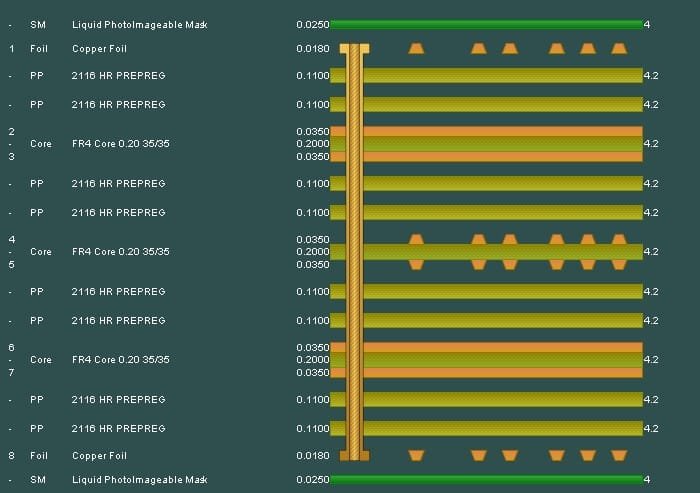

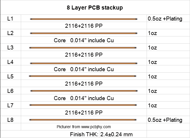
The above image explains the stack up in an 8-layer PCB. There are three cores in the PCB, and each core has two conductive layers. After every conductive layer, there is a prepreg layer for insulation. Finally, there is a surface layer at the top and one surface layer at the bottom. The components are placed on the surface layers only.
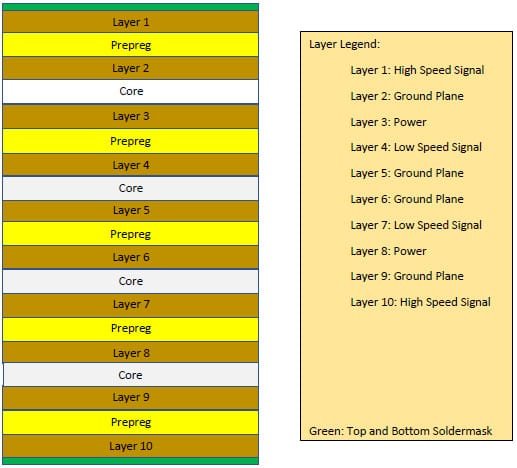
The stack-up remains the same in all multilayer PCBs; only the number of double-layer cores increases. Moreover, it is up to the user which layer he chooses for power, ground, signal, or any other purpose.
10 Layer PCB Stackup and Thickness
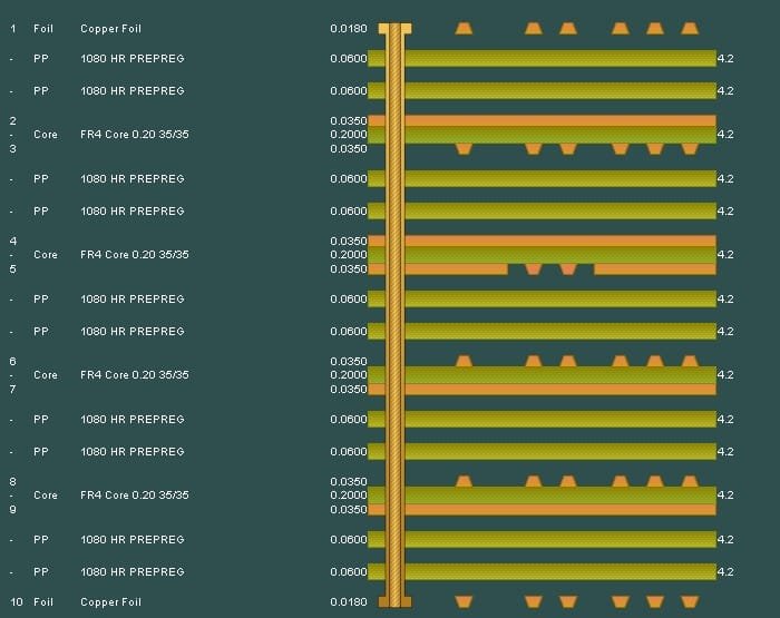
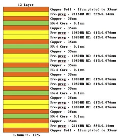
12-Layer PCB Stack-Up and Thickness
A 12-layer PCB includes five cores (ten inner layers) and two surface layers, supporting high-density designs for applications like data servers or aerospace systems. The stack-up follows a similar pattern to the 8-layer PCB, with additional cores and prepreg layers. The finished thickness typically ranges from 2.8–3.2 mm.
Design Consideration: Use inner layers for dedicated signal, power, or ground planes to optimize performance and minimize crosstalk.

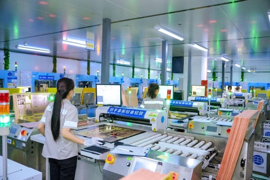
Multilayer PCB Manufacturing Process
Manufacturing multilayer PCBs requires precision and specialized equipment to ensure layer alignment, bonding, and quality. Below is a step-by-step overview of the process:
- Material Preparation:
- Common materials include FR-4, Rogers, Shengyi, and DuPont (for flexible PCBs). These materials are chosen based on dielectric properties, thermal resistance, and application needs. Learn more about PCB material selection.
- The lay-up operator places a copper foil and two prepreg sheets on a steel baseplate, followed by a pre-treated core aligned via pins.
- Stack Assembly:
- Additional prepreg and copper foil layers are added, with an aluminum press plate for a smooth finish. Up to three panels are stacked on the baseplate.
- The stack is pinned and moved to a hydraulic press with heated platens.
- Lamination:
- The press applies an initial “kiss” pressure of 50 psi, then heats to 350°F for at least one hour to cure the epoxy in the prepreg. Pressure bonds the layers, creating a permanent structure.
- The process is computer-controlled to ensure consistent heat and pressure. Complex PCBs (e.g., for defense applications) may include sub-assemblies with drilled and plated cores.
- Cooling and Unloading:
- The stack cools slowly to prevent warping, then is unloaded in a cleanroom. The lay-up operator removes the press plates and inspects the panels.
- The maximum board size is typically 12″ x 16″, with thicknesses ranging from 0.015″ to 0.125″.
For more step-by-step introduction to the PCB manufacturing process, please click here.
Recommended Reading
Multilayer PCB Manufacturing Videos
Quality Standards for Multilayer PCBs
Adhering to IPC standards ensures the reliability and performance of multilayer PCBs. Key standards include:
| IPC DOC# | ITEMS | Publication date |
| IPC-L-108 | Specification for Thin Metal Clad Base Materials for Multilayer Printed Boards | Jun-90 |
| IPC-L-109 | Specification for Resin Impregnated Fabric (Prepreg) for Multilayer Printed Boards | Jul-92 |
| IPC-CC-110 | Guidelines for selcting core constructions for multilayer printed wiring board applications | Dec-97 |
| IPC-TR-470 | Thermal Characteristics of Multilayer Interconnection Boards | Jan-74 |
| IPC-TA-721 | Technology Assessment Handbook on Multilayer Boards | |
| IPC-HM-860 | Specification for Multilayer Hybrid Circuits | Jan-87 |
| IPC-ML-960 | Qualification and Performance Specification for Mass Lamination Panels for Multilayer Printed Boards | Jul-94 |
| IPC-4101E | Specification for Base Materials for Rigid and Multilayer Printed Boards | Mar-17 |
Click here to learn more about PCB IPC standards.
How to Store Multilayer PCBs
Proper storage extends the shelf life of multilayer PCBs. According to IPC standards, PCBs should be vacuum-packed with foam cotton to prevent moisture and contamination. Store them in a dry, temperature-controlled environment to maintain quality.
Related Reading: How to Store PCB and PCBA?
Frequently Asked Questions (FAQs)
What is the difference between 4-layer and 8-layer PCBs?
A 4-layer PCB has one core (two inner layers) and two surface layers, suitable for simpler designs. An 8-layer PCB, with three cores, supports complex applications like medical or telecom devices, offering better signal integrity and power distribution.
How do I choose materials for multilayer PCBs?
Material choice depends on the application. FR-4 is cost-effective for general use, while Rogers or DuPont materials are ideal for high-frequency or flexible PCBs. Consult our material selection guide for details.
What are common challenges in multilayer PCB design?
Challenges include maintaining signal integrity, managing thermal dissipation, and ensuring layer alignment. Using dedicated ground planes and high-quality materials can mitigate these issues.
Conclusion
Building a multilayer PCB requires careful planning of the stack-up, precise manufacturing, and adherence to IPC standards. By understanding layer configurations, material choices, and quality control, you can design reliable PCBs for any application. Ready to start your PCB project? Explore our PCB manufacturing services or contact us for expert guidance.