Table of Contents
Why PCB Prototypes Matter
PCB prototypes are the foundation of electronic product development, allowing engineers to test functionality, identify design flaws, and optimize performance before mass production. Choosing the right PCB prototype service is critical to ensure quality, control costs, and meet project deadlines. Whether you’re designing a consumer gadget or a high-performance medical device, understanding key factors can make or break your project. In this comprehensive guide, we outline the essential considerations for ordering a PCB prototype service, from material selection to emerging trends, to help you achieve a seamless prototyping process. Let’s dive into the core factors that will guide your decision-making.
Core Factors for Choosing a PCB Prototype Service
1. Materials and Their Impact
Why It Matters
The PCB material determines electrical performance, thermal management, and durability. Selecting the right material aligns your prototype with project requirements and budget.
How to Choose
Common materials include:
- FR-4: The standard for most prototypes, offering a balance of cost, durability, and electrical performance.
- Polyimide: Ideal for flexible PCBs in wearables or foldable devices.
- Rogers: High-frequency material for RF and microwave applications.
- Kapton: Suited for high-temperature environments.
For most prototypes, FR-4 is sufficient due to its affordability and wide availability. However, advanced applications (e.g., 5G devices) may require Rogers for superior signal integrity.
Common Pitfall
Avoid choosing materials without consulting your manufacturer. For example, using Rogers for a low-frequency prototype unnecessarily increases costs.
Case Study: A drone manufacturer selected Polyimide for a flexible PCB prototype, enabling a compact design that reduced weight by 15% and improved flight efficiency.
2. PCB Layers and Complexity
Why It Matters
The number of layers impacts design complexity, cost, and lead time. Single-layer PCBs are simple and cost-effective, while multilayer boards (up to 32+ layers) support high-density designs.
How to Choose
- Single-layer: Best for basic circuits like LED drivers.
- Double-layer: Suitable for moderately complex designs.
- Multilayer: Essential for advanced applications like IoT devices or automotive electronics.
Prototypes often use fewer layers to speed up delivery. Copper, known for its high conductivity, is the primary conductive material.
Common Pitfall
Over-specifying layers increases costs and delays. Work with your manufacturer to optimize layer count. Explore PCB layer design tips.
3. Dimensions and Shape Optimization
Why It Matters
PCB size and shape affect manufacturing feasibility and cost. Smaller, rectangular boards minimize material waste and reduce expenses.
How to Choose
Check your manufacturer’s maximum board size (e.g., 500mm x 500mm at JHY PCB). Design compact layouts using PCB software to optimize space. Avoid irregular shapes unless necessary, as they increase production costs.
Common Pitfall
Oversized or irregular designs lead to higher costs, especially in bulk production. Test compact designs in the prototype phase to save money later.
Pro Tip: Use panelization techniques to maximize board usage. See JHYPCB’s design guidelines.
4. Thickness and Structural Integrity
Why It Matters
PCB thickness, ranging from 0.1mm to 8mm, affects mechanical strength and compatibility with components. Standard prototype thickness is 1.6mm for FR-4.
How to Choose
Thicker boards (e.g., 2mm) support heavy components, while thinner boards (e.g., 0.8mm) suit compact devices. Discuss thickness with your manufacturer to ensure structural integrity.
Common Pitfall
Specifying non-standard thickness without justification increases costs. Verify requirements early.
5. Trace Width and Spacing
Why It Matters
Trace width and spacing determine PCB compactness and electrical performance. Narrower traces enable denser designs but require advanced manufacturing.
How to Choose
JHY PCB supports minimum trace width and spacing of 2.5 mils. Wider traces reduce costs for prototypes, while tighter spacing suits high-density boards.
Common Pitfall
Overly tight spacing increases manufacturing complexity and cost. Balance density with budget.
6. Hole Types and Drilling Techniques
Why It Matters
Vias (for interlayer connections) and drilling holes (for components) impact functionality and cost. Minimum hole sizes vary by manufacturer.
How to Choose
Mechanical drilling is standard, but laser drilling offers precision for microvias in HDI boards. Confirm your manufacturer’s capabilities to match your design.
Common Pitfall
Specifying overly small holes without advanced drilling technology delays production.
7. Solder Mask and Surface Finish
Why It Matters
The solder mask prevents short circuits and protects copper traces, while surface finishes enhance solderability and prevent oxidation.
How to Choose
Solder Mask: Typically green, but available in white, blue, black, etc. Choose based on visibility and aesthetics.
Surface Finish: Options include:
Comparison Table
Surface Finish | Pros | Cons | Typical Use Case |
|---|---|---|---|
HASL | Low cost, good solderability | Uneven surface | General-purpose PCBs |
ENIG | Flat surface, excellent reliability | Higher cost | High-density boards |
Immersion Tin | Smooth, cost-effective | Tarnishing risk | Consumer electronics |
Immersion Silver | High conductivity | Tarnishing risk | High-frequency circuits |
Common Pitfall
Choosing premium finishes like ENIG for simple prototypes wastes budget. Explore surface finish options.
Case Study: A medical device company used ENIG for a high-density prototype, ensuring reliable soldering for critical components, reducing failure rates by 20%.
8. Copper Thickness and Electrical Performance
Why It Matters
Copper thickness (e.g., 1oz, 2oz) affects conductivity and heat dissipation. Standard prototype thickness is 1oz.
How to Choose
Thicker copper (e.g., 2oz) suits high-current applications, while 1oz is sufficient for low-power designs. Specify based on electrical needs.
Common Pitfall
Over-specifying copper thickness increases costs without benefit.
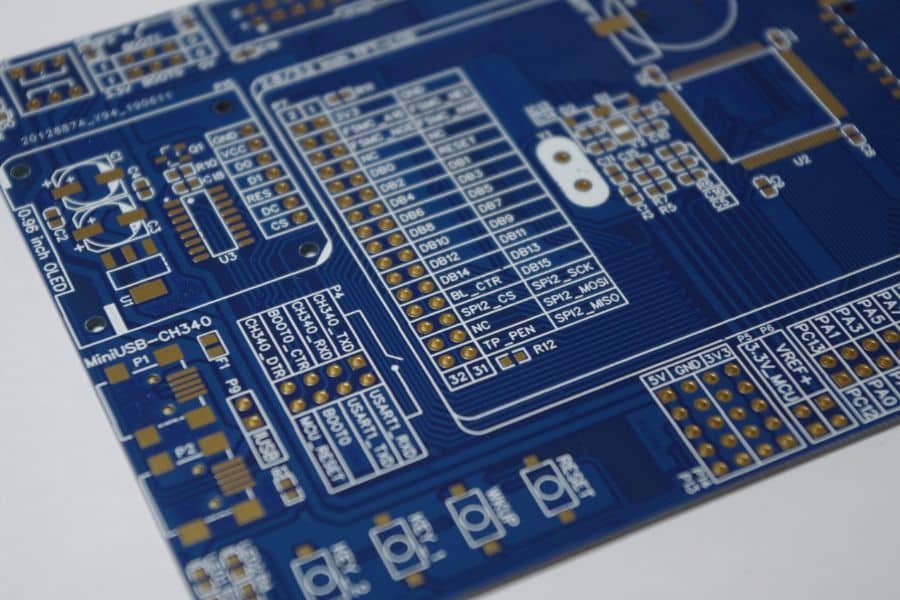
9. Silkscreen for Design Clarity
Why It Matters
Silkscreen labels components and test points, aiding assembly and testing. Standard colors are white, black, and yellow.
How to Choose
Ensure clear, legible printing for easy identification. Prototypes help evaluate silkscreen quality. Learn silkscreen best practices.
Common Pitfall
Overcrowded silkscreen reduces readability. Keep labels concise.
Practical Tools and Tips for Success
1. PCB Cost Estimator
Use an online tool to estimate costs based on layers, size, and finishes.
2. Design Checklist
Before ordering, verify:
- Material compatibility with project needs.
- Layer count aligns with design complexity.
- Dimensions fit manufacturer capabilities.
- Trace spacing and hole sizes meet design rules.
3. Choosing a Reliable Manufacturer
Evaluate suppliers based on:
- Lead Time: Look for fast turnaround (e.g., 24-48 hours for prototypes).
- Quality Certifications: IPC or ISO standards ensure reliability.
- Support: Choose manufacturers offering design reviews, like JHY PCB.
Tip: Request a sample prototype to assess quality before committing to bulk orders.
Emerging Trends in PCB Prototyping
The PCB industry is evolving to meet modern demands:
- High-Density Interconnect (HDI): Enables smaller, more complex boards for smartphones and IoT devices.
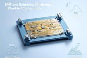
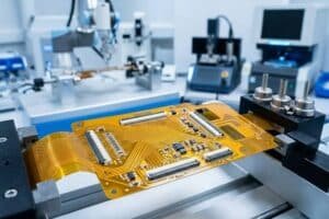
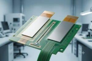
- Flexible PCBs: Growing in wearables and foldable electronics.
- Eco-Friendly Materials: Lead-free and recyclable options align with sustainability goals.
Partner with a manufacturer like JHYPCB that supports these trends to future-proof your designs.
Conclusion
Ordering a PCB prototype requires careful consideration of materials, layers, finishes, and more. By understanding these factors and leveraging tools like design checklists, you can optimize your prototype for performance and cost. Avoid common pitfalls like over-specifying features or neglecting manufacturer capabilities. Ready to start your project? Contact JHYPCB for fast, reliable, and customized PCB prototype services tailored to your needs.
Download our Free PCB Prototype Checklist to ensure a flawless ordering process!
Related Reading
- Custom PCB Manufacturing in Germany – Fast Prototype & Assembly Services
- Custom PCB Fabrication in China – Prototyping & Mass Production
- Expedited PCB Services – Quick Turnaround for Your Urgent Needs
- Rapid PCB Prototyping and Production – The Keys to Accelerating Your Product Launch
- Aluminum PCB Prototype: The Ultimate Guide for Engineers and Designers
- Fast and Reliable PCB Prototyping with JHYPCB in Australia
- Fast Prototype PCB Manufacturing Services in Canada by JHYPCB
- UK PCB Prototype Manufacturing: Fast, Affordable, and High-Quality
- Rapid PCB Prototyping Services: A Comprehensive Introduction
- Gerber Files for PCB Prototyping – A Comprehensive Guide
- Fast Prototype PCB Services for US Customers
- Choosing the Right PCB Material for Your Prototype: A Comprehensive Guide
- Why Should You Consider PCB Prototyping for Your Next Project?
- The Ultimate Guide to PCB Prototype Manufacturing: Everything You Need to Know
- What Are The Requirements To PCB Prototype Manufacturing?