PCBs are the backbone of electronic devices, and ensuring their quality is critical to performance and reliability. A poorly designed PCB can lead to malfunctions, costing time and money. This guide provides seven expert tips to evaluate PCB quality, whether you’re a designer ensuring signal integrity or a procurement manager selecting a reliable manufacturer. Follow these steps to identify high-quality PCBs and avoid costly mistakes.
Table of Contents

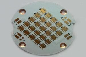
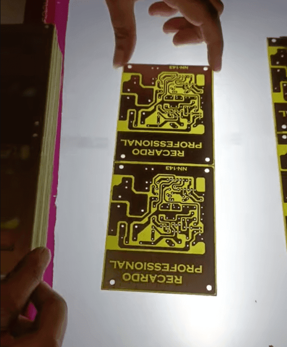
1. PCB Traces
Why Traces Matter
PCB traces are the conductive pathways that carry signals and power across the board. High-quality traces ensure reliable performance, especially in high-frequency or high-power applications like 5G devices. A protective solder mask prevents copper traces from oxidation or short circuits.
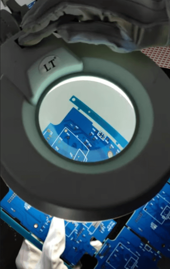
Also, check to see if all the traces are in a straight line, devoid of any bends. That is because bent lines could reduce the efficiency of such boards for high power & high-efficiency applications. You have to be extremely sure before you can accept PCBs with any kind of bends.
How to Check Trace Quality
- Solder Mask: Verify the solder mask is intact and uniformly applied. Green solder masks are preferred for their high visibility, making it easier to spot defects during visual inspection. White solder masks can obscure traces, complicating quality checks.
- Trace Alignment: Ensure traces are straight, with no bends. Bent traces can cause signal loss, reducing efficiency in applications like IoT or automotive electronics. For example, a bent trace in a 5G PCB may degrade signal integrity.
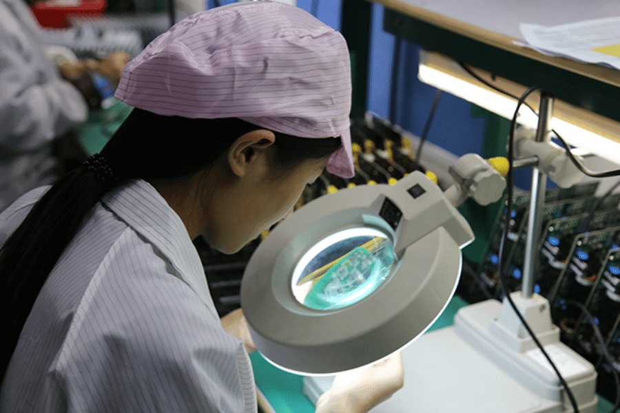
- Quick Tip: Use a magnifying glass to inspect trace alignment. Refer to IPC-A-600 standards for acceptable trace quality.
Learn More: Explore our PCB layout optimization guide for advanced trace design tips.
2. Decoupling Capacitors
Why Decoupling Capacitors Are Critical
Decoupling capacitors stabilize power delivery to chips, filtering out high-frequency noise that can disrupt performance. Proper placement is key to their effectiveness.
How to Verify Placement
- Proximity to Chips: Check that decoupling capacitors are placed close to the chip’s VDD pins, ideally within 1mm. Each VDD pin should have at least one capacitor to ensure stable power delivery.
- Impact of Poor Placement: If capacitors are too far, noise can interfere with chip performance, reducing PCB efficiency. For example, in a microprocessor PCB, distant capacitors may cause voltage drops, leading to system crashes.
- Quick Tip: Use a ruler or PCB design software to measure capacitor proximity. If capacitors are not adjacent to chips, the board design may be flawed.
3. Length of PCB Traces
Importance of Uniform Trace Lengths
In high-speed designs, such as those involving RAM or microprocessors, trace lengths must be equal to ensure synchronized signal arrival. Uneven lengths can disrupt timing, causing data errors.
How to Check Trace Lengths
- Measure Consistency: Use PCB design software or a ruler to verify that traces carrying related signals (e.g., data lines or clock signals) are of equal length.
- Application Example: In a DDR memory PCB, mismatched trace lengths can lead to signal skew, reducing memory performance.
- Quick Tip: Refer to IPC-2221 standards for trace length guidelines in high-speed designs.
4. Antenna Feedlines
Why Impedance Matching Matters
For PCBs with RF components (e.g., transmitters, receivers), the feedline connecting the RF chip to the antenna must match the antenna’s impedance (typically 50 ohms). Mismatched impedance reduces power transfer, limiting the device’s operating range.
How to Verify Feedline Quality
- Impedance Check: Ensure the feedline’s impedance matches the antenna’s using a network analyzer or PCB design software. For 5G or IoT devices, precise matching is critical for signal integrity.
- Visual Inspection: Confirm the feedline is free of sharp bends or irregularities that could disrupt impedance.
- Quick Tip: Use tools like Saturn PCB Toolkit to calculate feedline impedance.
5. Component Placement
Strategic Placement Rules
Component placement affects PCB performance and reliability. Improper placement can cause interference or inefficiencies.
How to Evaluate Placement
- Inductor Spacing: Ensure inductors are spaced apart to avoid magnetic coupling, which can alter their performance. Keep inductors away from metal objects to prevent induced currents.
- Exception for Toroidal Inductors: Toroidal inductors produce minimal external magnetic fields, so their placement is less critical.
- Functional Grouping: Components should be grouped by function (e.g., analog vs. digital sections) to minimize interference.
- Quick Tip: Use PCB design software to simulate component interactions. Refer to IPC-7351 standards for placement guidelines.
6. Trace Width & Routing
Why Trace Width Matters
Trace width must be sized correctly for the current it carries to prevent overheating or signal interference.
How to Check Trace Width
- Current Capacity: Use IPC-2221 standards to verify trace widths. For example, a 1A current typically requires a 0.5mm-wide trace on a 1oz copper PCB.
- Signal Type: Ensure traces for small analog signals are separated from fast-changing digital signals to avoid crosstalk. Inductor traces should not be overly wide to minimize RF emissions.
- Quick Tip: Use an online trace width calculator [link to tool] for precise sizing.
7. Grounds & Ground Planes
Importance of Ground Planes
A solid ground plane ensures stable voltage references and reduces noise in complex PCBs.
How to Verify Ground Quality
- 4-Layer Boards: For moderately complex PCBs, use a 4-layer board with inner layers dedicated to power and ground planes. Ensure the ground plane is continuous, except at the power supply’s negative terminal.
- Analog-Digital Separation: If the PCB has analog and digital sections, split the ground plane and connect it at the power supply’s negative terminal to prevent digital noise from affecting analog signals.
- Quick Tip: Use a multimeter to check ground plane continuity.
Quality Control in PCB Design, Manufacturing, and Testing
Ensuring PCB quality requires rigorous control across design, manufacturing, and testing phases.

Quality Control in PCB Design
- Correct Design Files: Verify schematic and layout files for accuracy using design rule checks (DRC).
- Manufacturability: Ensure the design adheres to the manufacturer’s capabilities (e.g., minimum trace width).
- Standardization: Follow IPC standards for consistent design practices.
- Testability: Include test points for easy inspection.
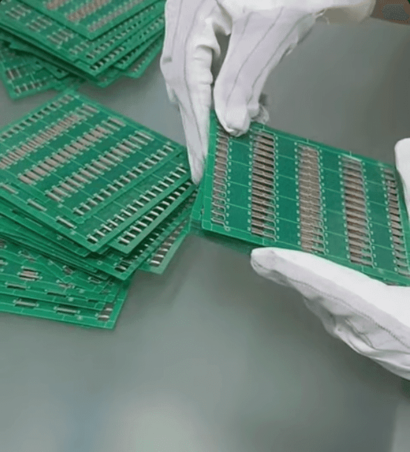
Quality Control in PCB Manufacturing
- Choose a Reliable Manufacturer: Select a manufacturer with ISO 9001 certification.
- Compliance: Ensure compliance with IPC, RoHS, and other regulatory standards.
- Pre-Production Checks: Review Gerber files before manufacturing begins.
- Process Control: Monitor critical steps like etching and soldering for consistency.
Quality Control in PCB Testing
Test PCBs using these methods to catch defects:
- In-Circuit Testing (ICT): Ideal for high-volume production to detect open circuits or incorrect components.
- Flying Probe Testing: Suitable for low-volume runs, offering flexibility without fixtures.
- Automated Optical Inspection (AOI): Detects soldering defects and component placement errors.
- X-ray Inspection: Identifies hidden defects like solder voids in BGA packages.
- Burn-in Testing: Stress-tests PCBs to ensure long-term reliability.
- Functional Testing: Verifies the PCB performs as intended in real-world conditions.
- Other Tests: Include soldering tests, contamination testing, and time-domain reflectometry (TDR).
Conclusion
High-quality PCBs are essential for reliable electronics, and knowing how to evaluate them saves time and costs. Use this checklist to ensure quality:
- Verify straight PCB traces with a green solder mask.
- Ensure decoupling capacitors are within 1mm of chip pins.
- Confirm equal trace lengths for high-speed signals.
- Check impedance matching for RF feedlines.
- Validate strategic component placement.
- Size trace widths per IPC standards.
- Use a continuous ground plane for 4-layer boards.
Whether designing your own PCB or partnering with a manufacturer, these tips will help you select reliable boards. For more insights, explore our PCB manufacturing resources or contact us at JHYPCB.
Related Reading
- 30 Common SMT PCB Assembly Defects
- Quality Control of Engineering Data for Multilayer PCB
- Angle Control in Multilayer PCB
- IPC Standards: A Guide to Standards for PCB Manufacturing and Assembly
- What Does PCB Open Circuit Mean?
- Why Should PCB Reliability Be Taken Seriously?
- Testing & Inspection Methods For PCB And PCBA
- Flying Probe Testing For PCB
- X-Ray Inspection In PCB Assembly