Table of Contents
Flexible PCB assembly requires more than simply placing components on a board. Because flexible circuits must balance electrical performance, mechanical stress, and handling stability, every step in the process can affect final reliability. In this guide, we’ll walk through the flexible PCB assembly process step by step and explain the key points buyers, engineers, and sourcing teams should pay attention to before production begins.
What Is Flexible PCB Assembly?
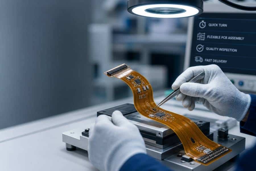
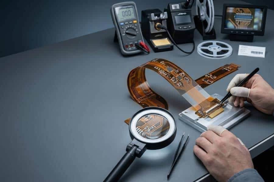
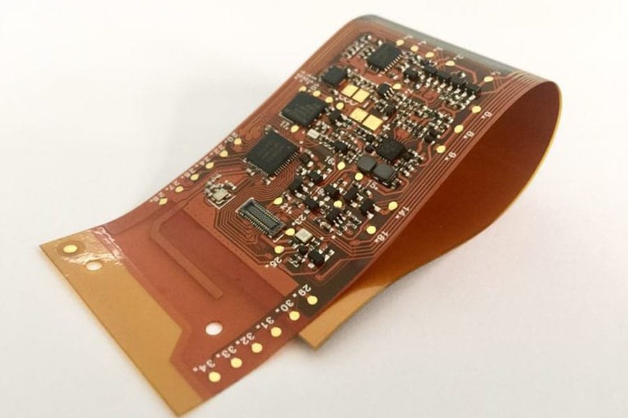
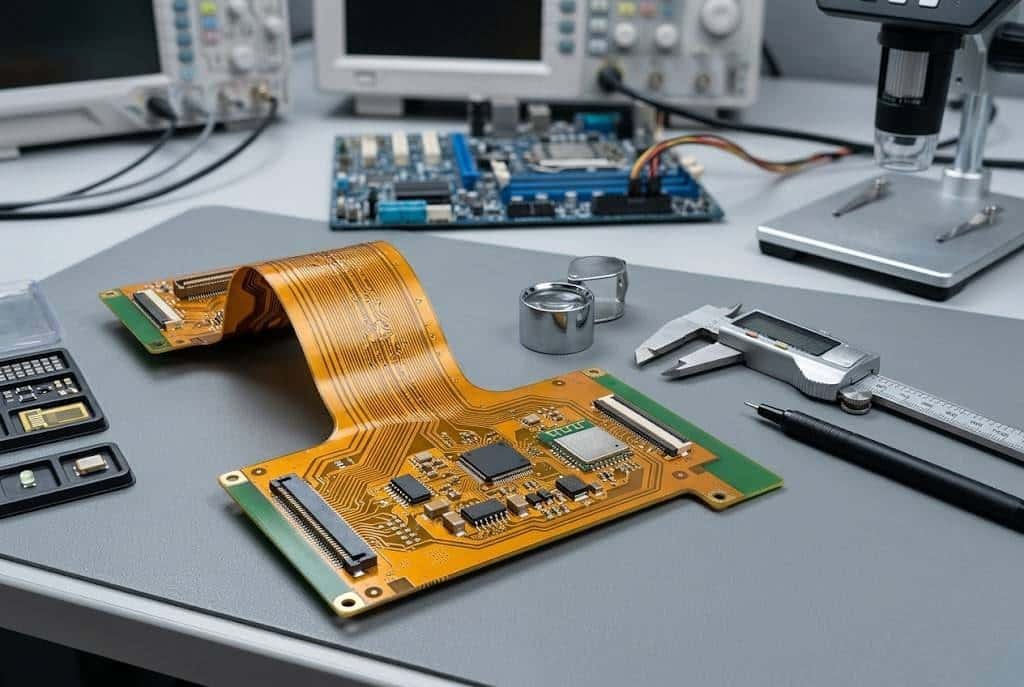
Flexible PCB assembly is the process of mounting electronic components onto flexible circuits such as polyimide-based boards. Unlike rigid PCB assembly, flex assembly has to account not only for solder quality and component placement, but also for board movement, mechanical stress, and support during processing.
Because flexible circuits can bend and shift more easily, the assembly workflow usually needs added handling controls such as carrier support, careful stencil alignment, controlled pick-and-place settings, and thorough inspection after soldering. In practice, that means the process is less forgiving than standard PCB assembly, and small issues in support, thermal control, or placement accuracy can affect yield and reliability.
For manufacturers and buyers, understanding this process matters because it helps set realistic expectations for design approval, tooling, lead time, and quality control. It also explains why flexible PCB assembly often requires closer coordination between engineering, production, and inspection teams before the first build starts.
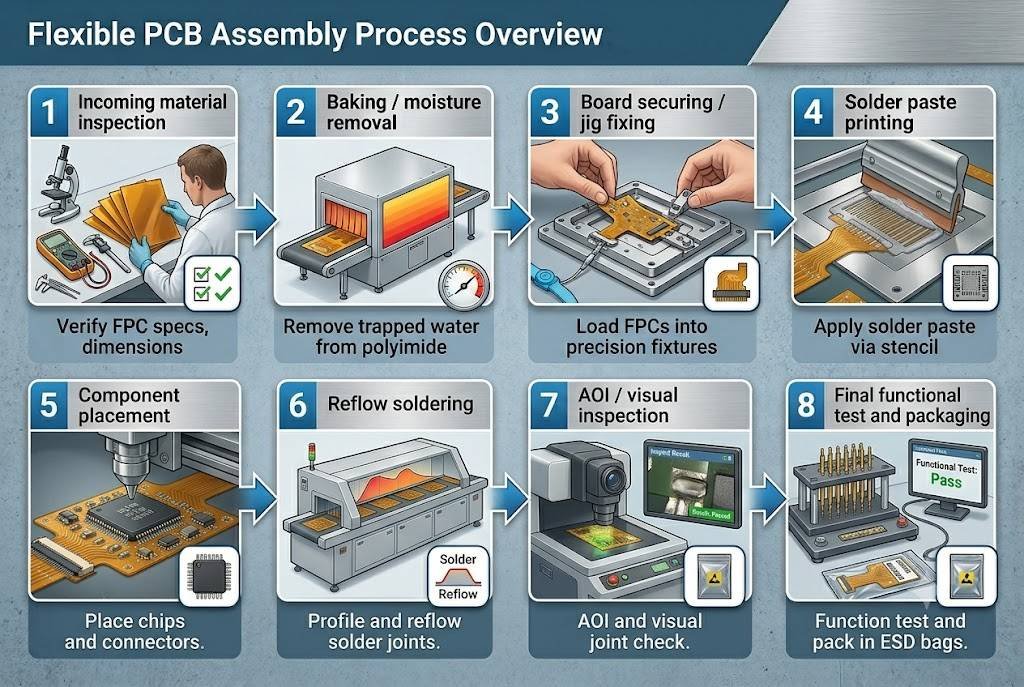
Flexible PCB Assembly Process Overview
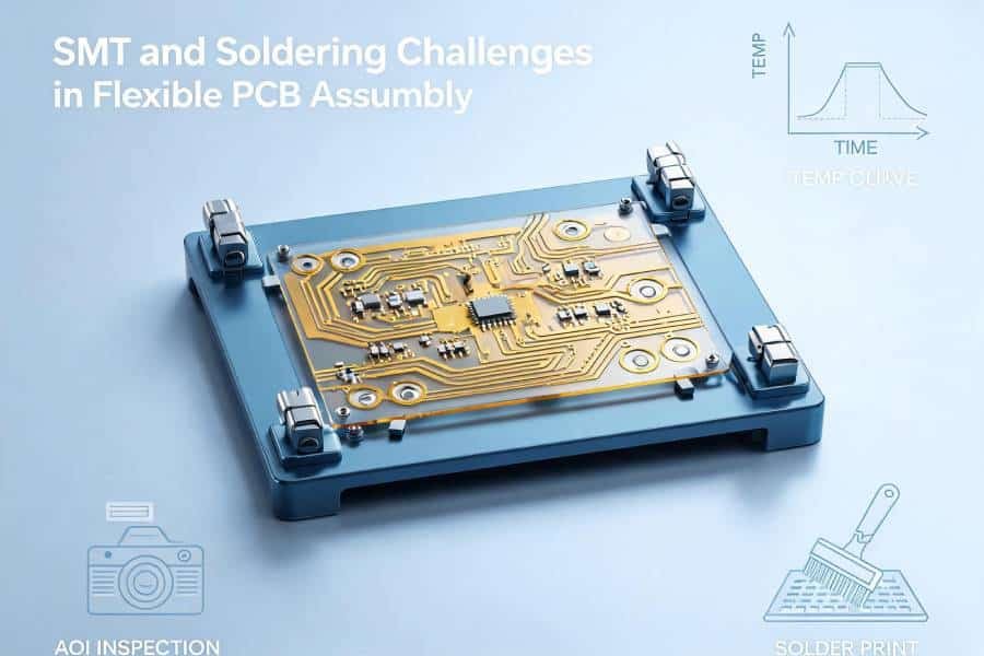
Flexible PCB assembly follows the same core SMT logic as rigid board assembly, but it requires tighter control at every stage because the board can flex, shift, or lose stability during processing. Manufacturers often rely on a carrier or fixture to keep the circuit flat during solder paste printing, component placement, reflow, and inspection.
Process flow list:
- Design and DFM review.
- Material and component preparation.
- Solder paste printing.
- Pick-and-place component assembly.
- Reflow soldering.
- Inspection and testing.
- Final cleaning, packaging, and shipment.
In some builds, extra steps may also be needed, such as stiffener installation, baking, or specialized test checks, depending on the board structure and end-use requirements. The main difference from rigid PCB assembly is not the sequence itself, but the need for better support, alignment, and process control to avoid movement, warping, and soldering defects.
Design and DFM Review
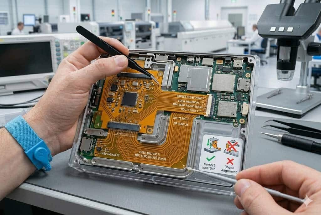
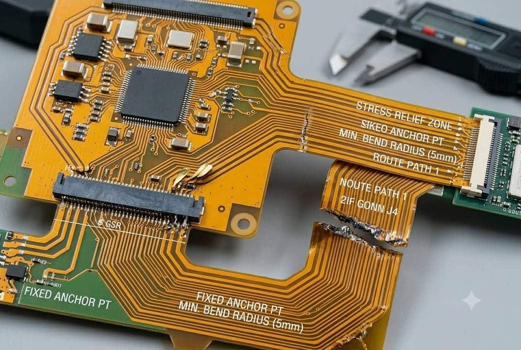
Before assembly begins, the design should be reviewed for manufacturability, assembly stability, and test access. For flexible PCB projects, this step is especially important because the board may need extra support, tighter tolerances, or special handling depending on where components are placed and how the circuit will be used.
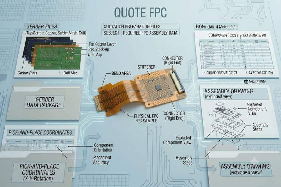
A strong DFM review usually checks whether the file package is complete, whether the board can be assembled without alignment problems, and whether the chosen materials and stackup support the intended process. For flex boards, that review often includes carrier or fixture needs, bend-area constraints, stiffener placement, fiducial locations, and whether any components should be moved away from dynamic flex regions.
If the design is not reviewed early, the risk of misalignment, solder joint stress, rework, and yield loss increases during production. That is why DFM is not just a technical checkbox; it is the point where the project becomes much easier to build reliably and much cheaper to produce at scale.
What DFM should confirm
- The Gerber, BOM, and assembly drawings are complete and consistent.
- Component placement avoids unnecessary stress in flex regions.
- Stiffeners are added where support is needed under components.
- Fiducials and tooling holes are positioned for reliable alignment.
- Test requirements are clear before the first build starts.
Material and Component Preparation
Once the design has passed DFM review, the next step is to prepare the materials, parts, and support hardware needed for assembly. For flexible PCB projects, this usually means confirming the flex substrate, coverlay, copper structure, stiffeners, and all components before the line starts.
A complete BOM is important, but it is not enough on its own. The assembly team also needs to verify component compatibility, package sizes, thermal tolerance, and whether certain parts should be mounted only in supported areas rather than in active flex zones. In many designs, stiffeners are added around connectors or component-heavy areas to improve rigidity and help the board survive printing, placement, and reflow.
At the same time, the carrier or fixture must be ready before SMT begins so the flexible circuit stays flat and properly aligned during processing. Proper preparation at this stage reduces handling errors, improves placement accuracy, and helps prevent defects caused by movement or uneven support.
What this stage should confirm
- The BOM is complete and matches the assembly drawing.
- All components are available and compatible with the flex design.
- The flex substrate and support materials match the process requirements.
- Stiffeners are installed where extra rigidity is needed.
- The carrier or fixture is ready for stable SMT processing.
Solder Paste Printing
Solder paste printing is the first critical SMT step in flexible PCB assembly. At this stage, the board must stay flat and stable so the paste is deposited only on the intended pads with the correct volume and alignment.
Because flexible circuits can shift or lift during printing, manufacturers typically mount them on a carrier or pallet before the stencil process begins. A precise stencil, accurate vision alignment, and controlled squeegee pressure are all important to keep paste deposits consistent and to reduce the risk of bridging, insufficient solder, or offset prints.
For fine-pitch parts, printing quality becomes even more important because small paste errors can quickly affect placement and reflow results. In practice, this means the print setup should be validated before full production starts, especially when the flex design includes thin traces, dense component layouts, or areas that are difficult to support evenly.
Key printing checks
- The flex board is fixed to a carrier or pallet before printing.
- The stencil matches the pad layout and paste volume requirements.
- Fiducials are aligned accurately before paste deposition.
- The squeegee pressure is controlled to avoid uneven release.
- The printed paste is inspected before the board moves to placement.
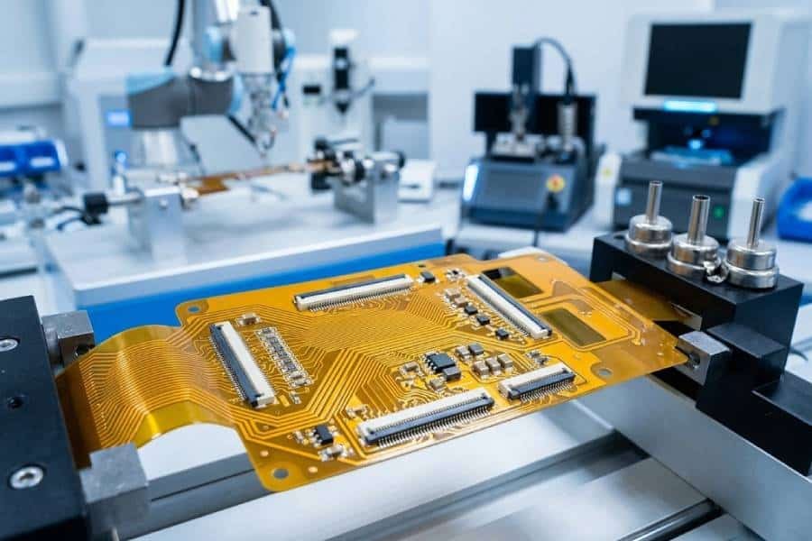
Pick-and-Place Component Assembly
After solder paste printing, components are placed onto the flexible PCB using SMT pick-and-place equipment. In flex assembly, the goal is not only accurate placement, but also stable handling, because the board can move or bounce if the support system is not secure enough.
To reduce shifting, the flexible circuit is usually kept on a rigid carrier or pallet during placement. This support helps the machine maintain alignment while the vision system locates fiducials and places parts at the correct coordinates. Placement settings also matter: nozzle pressure, speed, and pick height need to be tuned so the board is not distorted and the components are not damaged.
Component orientation and location are especially important on flexible boards, since parts placed too close to bend areas can experience added mechanical stress later in use. For that reason, assembly teams often verify the board layout again before placement begins, especially when the design includes fine-pitch parts, dense layouts, or stiffener-supported zones.
What this stage should verify
- The board is firmly fixed to a carrier or pallet.
- Fiducials are visible and correctly aligned.
- Placement force and speed are set for flex material.
- Sensitive parts are not placed in active bend zones.
- Component orientation matches the assembly drawing and process plan.
Reflow Soldering and Thermal Control
Reflow soldering is where the solder paste is heated until it melts and forms the final electrical and mechanical joints. For flexible PCB assembly, this step must be controlled more carefully than standard rigid board reflow because thin substrates can deform, shift, or respond unevenly to heat.
The reflow profile should be tuned to the board’s material, thickness, component density, and solder paste specification. In practice, manufacturers usually aim for a controlled ramp-up, a stable soak period, and a peak temperature that stays as low as possible within the paste’s recommended range to reduce thermal stress. Using a proper carrier or fixture helps keep the board flat during heating and reduces warpage as the assembly moves through the oven.
Thermal profiling is especially important when the layout includes stiffeners, heavy components, or mixed thermal masses, because those areas may heat at different rates. If the profile is too aggressive, the board may bow, pads may lift, or components may shift before the solder solidifies. That is why flex assemblies often need process validation before production, not just a default rigid-board oven setting.
Key thermal checks
- Use a reflow carrier or pallet to keep the board flat.
- Set a flex-specific profile instead of using a rigid-board default.
- Control ramp-up speed and cooling rate to reduce stress.
- Validate the profile with thermocouples on the board.
- Watch for warpage, delamination, and component shift after reflow.
Inspection and Testing
Inspection and testing are used to confirm that the flexible PCB assembly meets quality and functional requirements before it leaves the factory. Because flex boards can be more delicate than rigid boards, manufacturers usually combine visual inspection with electrical or functional checks to catch both surface defects and hidden problems.
AOI is commonly used to identify missing parts, misalignment, solder bridges, and other visible defects after assembly. For denser layouts or hidden solder joints, X-ray inspection can help detect voids, bridging, or internal solder issues that are not visible from the outside. In some projects, especially prototypes and low-volume builds, flying probe, ICT, or functional testing may also be used depending on how much electrical coverage is needed.
For flex assemblies, additional checks may be needed when the product will be bent, touched, or used in demanding environments. These can include bend testing, solder joint strength checks, or project-specific functional tests designed with the customer’s end use in mind. The goal is not only to find defects, but also to confirm that the assembly will keep performing after handling, installation, and real-world use.
Typical test methods
- AOI for visible placement and solder defects.
- X-ray for hidden joints and internal solder issues.
- ICT or flying probe for electrical verification.
- Functional testing for real-use performance.
- Special mechanical or bend tests when the application requires it.
Final Cleaning, Packaging, and Shipment
After the assembly has passed inspection and testing, the final step is to clean, protect, and package the boards for delivery. Flexible PCBs are especially sensitive to pressure and bending, so the packaging method should keep the assembly flat and stable from the factory to the customer’s receiving dock.
For populated boards, anti-static packaging is typically used to reduce the risk of ESD damage during shipping and storage. Moisture-sensitive or polyimide-based flex assemblies may also be sealed with desiccant in a moisture-resistant bag before being placed into a cushioned outer box. When the boards are stacked, they should be separated or supported so that connectors, stiffeners, or small components are not crushed or bent.
Good packaging also helps preserve solder joint quality and surface condition after assembly, especially when the parts will be shipped long distances or stored before final use. In other words, packaging is not just a logistics step; it is part of the quality-control process for flexible PCB assembly.
Packaging checks
- Use anti-static or shielding bags for populated assemblies.
- Add desiccant when moisture protection is needed.
- Keep the board flat with trays, inserts, or rigid support.
- Avoid pressure on connectors, stiffeners, and delicate parts.
- Confirm the outer box provides enough cushioning for transport.
Common Challenges in Flexible PCB Assembly
Flexible PCB assembly has a few recurring failure modes that are less common in rigid board production. The most frequent problems include warpage, component misalignment, solder joint stress, pad lifting, and cracks that appear after bending or thermal cycling.
Handling and alignment are especially sensitive because the substrate can stretch, flex, or shift during printing, placement, and reflow. If the board is not properly supported, even a small amount of movement can lead to print offset, poor wetting, or displaced components. Thermal stress is another major issue, since flex materials and copper can expand differently during heating, which increases the risk of warpage and solder joint damage.
Long-term reliability is also a concern when parts are placed too close to bend zones or when the board is repeatedly flexed after assembly. In those cases, traces, joints, and transition areas may develop fatigue or cracking over time. That is why successful flex assembly depends on both good process control and good design discipline.
Common problems to watch
- Warpage during printing or reflow.
- Solder bridges or weak solder joints.
- Component misalignment during placement.
- Pad lifting or trace cracking under stress.
- Early failures caused by poor bend-zone layout.
How to Improve Assembly Success
The best way to improve flexible PCB assembly success is to control problems before production starts. That means reviewing the design early, confirming material choices, stabilizing the board during SMT, and validating the thermal profile before the first full run.
A strong flex assembly workflow usually combines DFM review, proper support tooling, process control, and inspection. Early collaboration with the manufacturer helps catch layout issues, component placement risks, and support requirements before they turn into rework or scrap. On the production side, carriers, fixtures, and controlled reflow profiles help reduce movement and thermal stress, while AOI, X-ray, and electrical testing catch defects early.
It also helps to choose components and layouts that respect the mechanical nature of flex circuits. Low-profile parts, sensible placement away from bend areas, and clear documentation for tooling and test needs all contribute to better yield and more consistent results. In short, the more predictable the process is from design through shipment, the easier it is to build a reliable flex assembly at scale.
Practical ways to improve yield
- Run a DFM review before releasing files to production.
- Use carriers or fixtures to keep the board flat through SMT.
- Validate the reflow profile for the specific flex build.
- Inspect with AOI and X-ray before shipment.
- Keep components, bend zones, and stress areas well planned in the layout.
When to Contact a Flexible PCB Assembly Partner
You should contact a flexible PCB assembly partner when the project moves from general planning to real manufacturing decisions. That usually includes cases where you need a DFM sanity check, help with materials or stiffeners, guidance on bend areas, or support deciding whether the design is ready for production.
It is also the right time to reach out when the project has special requirements such as tight lead time, complex component placement, mixed rigid-flex construction, or a need for testing beyond standard inspection. In those situations, a quick review can help prevent quoting mistakes, reduce revision cycles, and avoid delays later in CAM, tooling, or incoming inspection.
For buyers, engineers, and sourcing teams, the best practice is to share the design files early and ask for feedback before the first build starts. That usually means Gerbers, BOM, assembly drawings, and any notes about bend constraints, test needs, or special process requirements. The earlier the communication starts, the easier it is to align cost, lead time, and reliability expectations.
Use this stage when
- You need a DFM review before releasing files.
- You are unsure about stiffeners, bend zones, or support tooling.
- Your board needs custom testing or special handling.
- You want a quote for prototype or production assembly.
- You need help confirming whether the design is manufacturable.
Conclusion
Flexible PCB assembly is not just a smaller version of rigid PCB assembly; it is a process that depends on careful design review, stable support, controlled printing and placement, precise thermal management, and thorough inspection. When each stage is handled with the right tooling and process discipline, flex assemblies can deliver strong reliability and consistent production results.
If your project involves bend zones, stiffeners, dense SMT layouts, or special testing requirements, it is worth bringing in an experienced flexible PCB assembly partner early. Sharing your Gerbers, BOM, and assembly notes before production starts can help reduce risk, improve yield, and make quoting and scheduling more accurate.
Ready to move forward? Contact our team for a flexible PCB assembly quote or technical review, and we’ll help you evaluate the design before the first build begins.
FAQs
Flexible PCB assembly is the process of mounting and soldering components onto a flexible circuit board. Compared with rigid PCB assembly, it requires more careful handling, better support tooling, and tighter thermal control to avoid movement and damage during production.
A carrier or fixture keeps the flexible board flat and stable during solder paste printing, component placement, reflow, and inspection. Without that support, the board can shift, warp, or become harder to align accurately.
Lorem ipsum dolor sit amet, consectetur adipiscing elit. Ut elit tellus, luctus nec ullamcorper mattis, pulvinar dapibus leo.
You should usually send Gerbers, BOM, assembly drawings, and any notes about bend areas, stiffeners, test requirements, or special process needs. Including target lead time also helps the supplier quote more accurately.
No, but they are often used when a design needs extra rigidity under connectors, fine-pitch parts, or other stress-sensitive areas. Stiffeners help the board stay flat during SMT and reduce bending stress after assembly.
Common testing methods include AOI, X-ray, ICT, flying probe, and functional testing. Depending on the application, additional checks such as bend testing or thermal stress testing may also be used.
Typical defects include warpage, component misalignment, solder bridges, weak joints, pad lifting, and cracks caused by bending or thermal stress. Good DFM, stable support, and proper thermal profiling help reduce these risks.
Lead time depends on complexity, material availability, testing requirements, and order volume. Simple flex builds may move quickly, while rigid-flex or more complex projects usually take longer.
You should reach out when the design needs DFM review, special bend-area guidance, stiffener decisions, or custom testing support. It is also a good idea to contact a partner early if you want a more accurate quote and fewer revisions before production starts.