SMT and Soldering Challenges in Flexible PCB Assembly: A Process Engineer’s Guide

Flexible PCBs are far more demanding than FR4 boards during SMT and soldering. This article, written from a process engineer’s perspective, explains the key challenges in flex PCB assembly—including warpage, solder paste printing, reflow profiling, bending‑area reliability, and inspection—and outlines practical, production‑ready countermeasures to stabilize yield before mass production.
Cover image showing a flexible PCB clamped on an SMT carrier fixture, illustrating SMT and soldering challenges in flexible PCB assembly.

Table of Contents

Flexible PCBs bring clear advantages in weight, space saving, and dynamic bending, so they are widely used in cameras, wearables, medical devices, and compact consumer electronics. However, the same thin, bendable polyimide or PET structure that helps product design also makes SMT and soldering much more sensitive to process variation than on standard FR4 boards.

From a process engineer’s perspective, flexible PCB assembly is not just “copy FR4 parameters to a softer board”. Warpage, dimensional changes, unstable support, and narrow thermal windows can easily turn small deviations in printing, placement, or reflow into large yield and reliability problems. This article focuses on those SMT and soldering challenges and the practical countermeasures you can apply on the line, so that most potential failures are controlled at the process window stage instead of being discovered after field returns.

Challenge 1 – Warpage and Dimensional Stability of Flex PCB Panels

Why warpage is more serious on flexible PCBs

Compared with rigid FR4, flexible substrates such as polyimide are much thinner, have lower stiffness, and respond more strongly to temperature and mechanical stress. Even small changes in oven temperature, clamping force, or handling can cause local bending or global warpage on the panel during SMT.

In reflow, the combination of copper, adhesives, coverlay, and stiffeners with different coefficients of thermal expansion (CTE) makes the flex panel expand and shrink unevenly. If the panel is not properly supported, this expansion mismatch tends to concentrate at component areas, leading to bending under BGAs, QFNs, and fine‑pitch ICs at exactly the moment when solder is molten and joints are most vulnerable.

How warpage and dimensional changes affect SMT and soldering

On the printing and placement stages, insufficient flatness leads to three typical issues:

  • The flex panel may sag or vibrate on the conveyor, causing component placement shift or rotation, especially for small passives and fine‑pitch ICs.
  • Contact between stencil and board surface becomes inconsistent, so solder paste thickness varies across the panel.
  • Fiducial recognition and alignment accuracy degrade if the panel stretches or shrinks beyond the machine’s compensation range.

During reflow, warpage can lift component corners, making some pads partially or completely lose contact with molten solder and resulting in opens, head‑in‑pillow, or weak joints. In extreme cases, repeated heating cycles or excessive mechanical constraint from misdesigned fixtures may cause pad cratering or trace cracking near large components.

Process engineering countermeasures: fixtures, carriers, and panel design

Illustration comparing flex PCB warpage during reflow without a carrier versus flat behaviour on a rigid carrier fixture.

To keep flexible PCBs under control, most successful SMT lines treat them as a “semi‑rigid system” by combining them with carriers, stiffeners, or panel frames.

Key actions you can take as a process engineer include:

  • Use FR4 carriers or panel frames: Attach individual flex circuits to a rigid backing panel so that the SMT line sees a flat, rigid unit for printing, placement, and reflow.
  • Design fixtures with proper material and CTE: Choose carrier materials with adequate heat resistance and a thermal expansion behavior close to that of the flex assembly to minimize additional stress during reflow.
  • Optimize fixation and locating features: Use well‑designed tooling holes, edge rails, vacuum cavities, and clamps to secure the flex without creating local stress points that could imprint or damage the copper and coverlay.
  • Measure and monitor warpage: Include warpage checks in your first‑article inspection and periodic in‑process audits, using a height gauge or 3D measurement where available, and tie those measurements back to carrier design and oven profiles.

When warpage and dimensional stability are addressed at the panel and fixture level, the rest of the SMT process—stencil design, printing parameters, and placement—becomes much easier to stabilize, and many downstream soldering defects are prevented before they appear.

For projects that need carrier and panel design support, our flexible PCB assembly services team can co‑engineer fixtures and panelization with you from the prototype stage.

Challenge 2 – Solder Paste Printing on Flexible Substrates

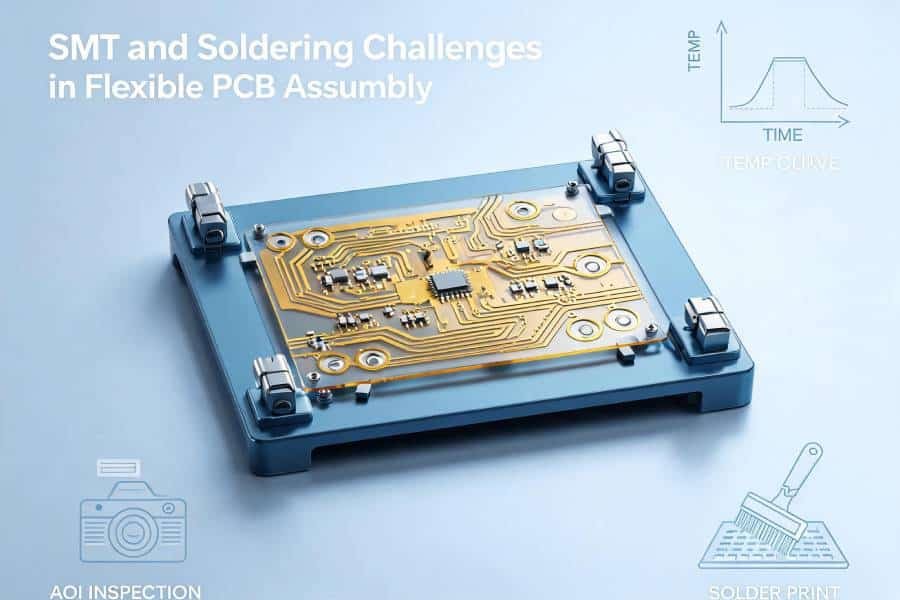
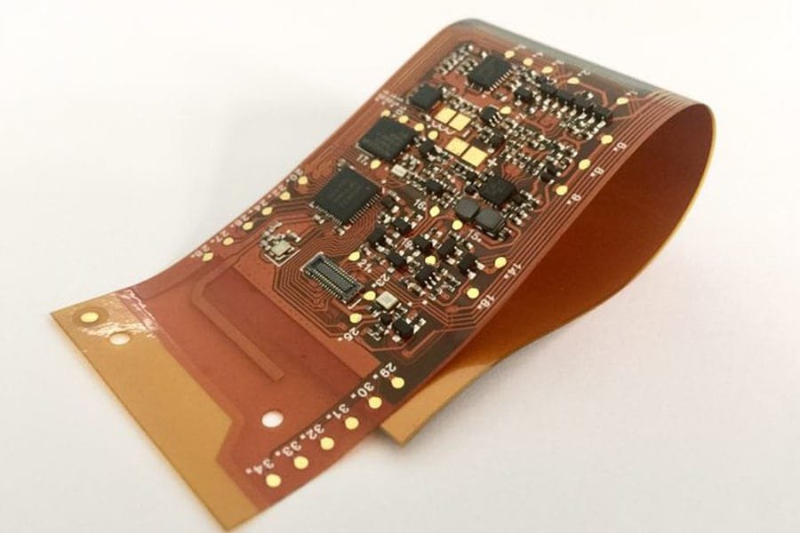
Compared with rigid FR4 panels, solder paste printing on flexible PCBs is fundamentally more unstable because the substrate does not stay perfectly flat during clamping and printing. Even a small amount of flex or sagging changes the contact condition between stencil and board, which directly affects paste transfer efficiency and volume consistency, especially for fine‑pitch ICs and dense connector areas. As a result, many classic SMT defects on flex—bridging, insufficient solder, smeared deposits, and misalignment—can often be traced back to the printing stage rather than to placement or reflow alone.

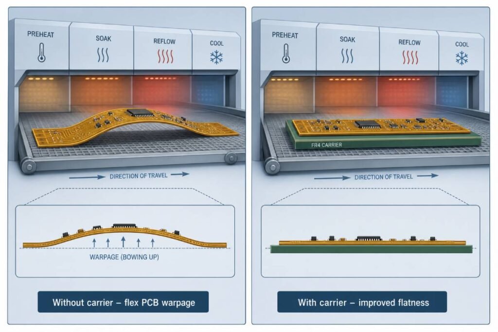
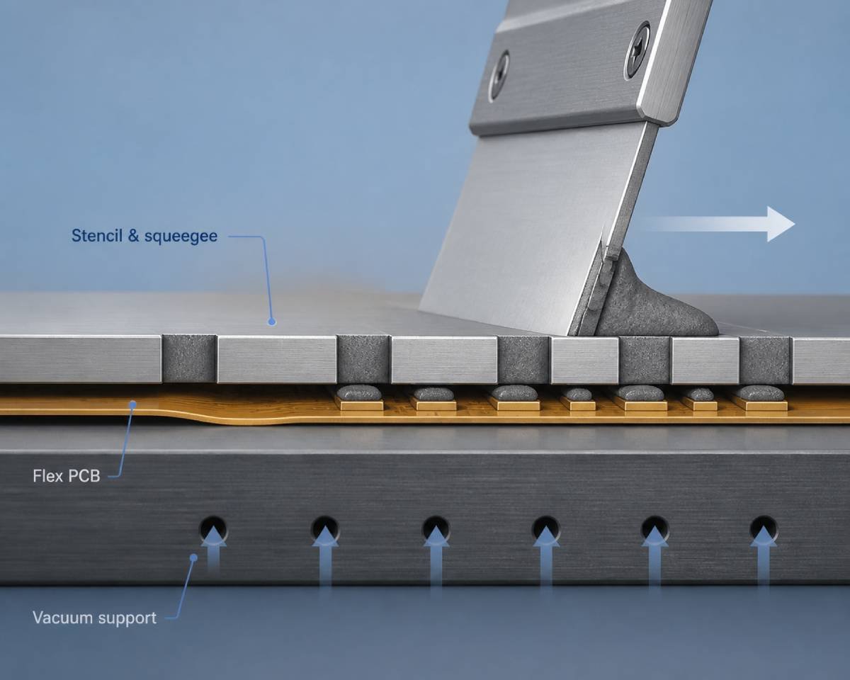
From a process engineer’s standpoint, the first priority is mechanical stabilization of the flex during printing. Ideally, the FPC should be fully supported from the bottom with a dedicated support plate, vacuum tooling, or a carrier that brings the assembly close to a rigid‑board behavior in the Z‑direction. Vacuum support fixtures or vacuum print support plates create a uniform backing under the entire image area so that the stencil can gasket properly against the copper pads, reducing local gaps that would otherwise cause uneven paste thickness and slumping. For thinner flex or mixed‑density designs, magnetic or pin‑based carriers can also be used, but process engineers must verify that there are no unsupported “islands” under critical components where the board can flex during squeegee travel.

Cross-sectional schematic of solder paste printing on a flexible PCB fully supported by a vacuum fixture, showing stencil and squeegee.

Stencil and aperture design become the next key control dimension once the board is mechanically stable. For fine‑pitch packages around 0.5 mm and below, thinner stencils and carefully reduced aperture sizes help keep the area ratio within a good transfer window and reduce bridging risk. Step‑down regions or step stencils are often needed when large power pads or connectors coexist with small IC pads on the same flex, allowing reduced thickness in fine‑pitch zones while still delivering enough volume to large pads. Standard guidelines such as moderate aperture reduction, rounded corners, and segmented openings for large thermal pads are still valid on flex, but process engineers should pay extra attention to paste release in apertures located over any region that could still exhibit slight bowing.

Printing parameters also need tighter control than on rigid boards. Excessive squeegee pressure may seem to improve gasketing, but on a flexible panel it can actually deform the substrate, causing smear and variable deposit heights across the stroke. Instead, process engineers should tune squeegee speed, pressure, and separation speed together, aiming for just enough force to ensure full aperture filling and clean wipe without visibly bending the panel. Consistent stencil cleaning intervals and the use of solder paste grades suitable for fine‑feature printing further reduce variability, especially when area ratios are pushed toward the lower acceptable limit.

Finally, it is important to close the loop between design and process. Adding robust fiducials and precise tooling holes on the flex allows the stencil printer’s vision system and mechanical clamping to work reliably, even when the panel outline is complex. When process engineers observe systematic paste‑related defects confined to certain zones on the flex, this feedback should be translated into concrete DFM recommendations: adjusting pad sizes, redistributing dense fine‑pitch components away from bend lines, or modifying stiffener layout to provide better support under the most critical printing areas. With this collaborative approach, many seemingly “random” soldering issues on flexible PCBs can be eliminated already at the paste printing stage rather than being treated later as reflow or inspection problems.

For a broader overview of stencil types and solder paste selection in SMT, see our SMT stencil and solder paste printing guide.

Challenge 3 – Reflow Soldering Profile and Heat Sensitivity

Reflow is often where flexible PCB assemblies either succeed or completely fail, because thin polyimide stacks heat up and cool down much faster than traditional FR4 boards. With less thermal mass and more compliant adhesive systems, flex circuits are far more vulnerable to blistering, delamination, discoloration, and warpage if a “rigid‑board style” profile is applied without adjustment. At the same time, insufficient heat or poorly controlled ramps can cause cold joints, incomplete wetting, or head‑in‑pillow defects on fine‑pitch and bottom‑terminated components. For process engineers, the challenge is to find a narrow thermal window that fully reflows the solder while keeping both the flex substrate and sensitive components within their safe limits.

One key difference is that flexible circuits, especially simple one‑ or two‑layer designs, reach target temperatures much quicker than thicker rigid or rigid‑flex boards. This means that a reflow recipe copied directly from a thick FR4 assembly will often expose a flex PCB to unnecessarily long times above liquidus and higher peak temperatures than needed, accelerating moisture outgassing and mechanical stress in the adhesives and coverlay. Good practice is to start with lower ramp rates, shorter overall time in the reflow zone, and a peak temperature that still meets the alloy requirements but stays as low as possible within the process window, typically ensuring a controlled rise of no more than about 2 °C per second and limiting the time above liquidus to what is strictly necessary.

Because warpage is a dominant failure driver for flex during reflow, mechanical support strategies from the printing and placement stages should be maintained through the oven whenever possible. Synthetic stone or high‑temperature composite carriers can clamp thin or flexible boards along their edges and provide distributed support under the main circuit area, preventing sagging as the substrate softens at high temperatures. When designing these pallets, process engineers should aim to minimize the temperature difference between the board and the fixture, keep the clearance between PCB edge and pallet edge small, and provide enough central support so that the panel does not bow between contact points at peak temperature. Profiling must then be performed with thermocouples attached both to the flex circuit and, where relevant, to the carrier, to ensure that the chosen recipe achieves full solder reflow without creating excessive thermal gradients across the assembly.

Moisture management is another critical factor that interacts directly with reflow profiling on flex PCBs. Once a flexible circuit has absorbed moisture from ambient storage, rapid heating in the oven can cause steam expansion inside the stack‑up, leading to blisters, delamination, or localized bulging of the coverlay. To reduce this risk, process engineers should define and enforce appropriate baking conditions for flex panels before reflow, taking into account thickness, material system, and previous exposure history. Combined with a profile that avoids overly aggressive ramps and peak temperatures, this preconditioning step significantly improves the odds of preserving both cosmetic appearance and long‑term reliability of solder joints and dielectric layers on flexible PCB assemblies.

For general guidance on lead‑free reflow curves in SMT, you can also read our reflow soldering temperature profile guide.

Challenge 4 – Component Layout and Mechanical Stress in Bending Areas

Even with a perfect reflow profile and stable fixturing, flexible PCB assemblies can still fail prematurely if components and solder joints sit in areas that will bend during product use. When a flex region is repeatedly bent or twisted, the copper traces, pads, and solder joints in that zone experience cyclic mechanical strain, which can lead to cracked solder joints, pad lifting, or even broken conductors over time. For process engineers, these failures often show up later as “mysterious” intermittent faults, yet their root cause lies in how components and stiffeners were placed relative to the bending zones.

From a manufacturing and DFM perspective, the first rule is straightforward but frequently violated: do not place components, vias, or through‑holes directly in active bending areas. Industry design guides consistently recommend keeping critical components and interconnects a safe distance away from the bend line and maintaining an appropriate minimum bend radius based on layer count and flex thickness. Where miniaturization forces components to be near a flex‑to‑rigid transition or in a region that will experience occasional bending, process engineers should push for the use of stiffeners (FR4, PI, or metal) to locally restrict flexing and shift mechanical stress away from the solder joints.

Stiffener design itself strongly influences long‑term solder joint reliability. A good stiffener should extend beyond the exposed coverlay area and overlap by a small margin so that bending stress is gradually transferred from the rigid stiffener to the flexible circuit, instead of concentrating exactly at the pad edge. Guidelines also suggest avoiding stiffener edges directly under or immediately adjacent to component pads and ensuring that stiffener thickness and adhesive systems are compatible with the SMT process and connector insertion forces. For connectors or switches that see significant mechanical loading, the stiffener should cover the entire footprint and include secondary anchoring features so that mating or actuation forces are borne mainly by the mechanical stack‑up rather than by the solder joints alone.

Routing and pad design in bending regions is another area where process engineers can provide targeted feedback to design teams. Trace paths in flex zones should use smooth curves rather than sharp 90‑degree corners, and adjacent‑layer traces should be staggered instead of stacked directly on top of each other to avoid creating stiff “spines” that concentrate strain. Vias and test pads should be kept out of high‑strain regions as much as possible, and any necessary copper features near bends may need wider pads, teardrop fillets, or special pad shapes to distribute stress more evenly. By turning typical failure findings—like cracked joints at the edge of a stiffener or broken traces along a bend—into concrete, documented layout rules, process engineers can significantly reduce field returns and improve the robustness of flexible PCB assemblies under real‑world mechanical loads.

For more detailed discussions on flex PCB stiffener materials, thickness selection, and SMT area design, see our flex PCB stiffener design guidelines.

Challenge 5 – Inspection, Testing, and Handling in SMT Lines

Inspection and testing on flexible PCB assemblies are not just “copy‑paste” from rigid boards, because the substrate’s tendency to bend, stretch, or wrinkle changes how AOI, X‑ray, ICT, and FCT fixtures behave. If the flex is not properly supported and constrained during inspection, apparent defects may simply be image distortion or misregistration, while real defects can be missed because solder joints and pads are not presented consistently to cameras and probes. At the same time, excessive manual handling between inspection and test steps increases the risk of creases, micro‑cracks, or connector damage on already‑assembled flexible circuits.

For AOI, the primary challenge is dimensional deformation of the flex panel between the “golden board” reference and the actual production boards. Small shifts in pad location due to stretching or panel bowing can confuse standard AOI algorithms, causing high false‑call rates unless the system and fixtures are tuned specifically for flex. Process engineers can mitigate this by using rigid carriers or vacuum plates to hold the flex flat during image capture, and by configuring AOI programs with more tolerant global and local alignment strategies that account for minor dimensional changes while still keeping tight thresholds on critical solder joints. In practice, it often makes sense to prioritize AOI coverage on high‑risk areas—fine‑pitch ICs, dense connector zones, and bending‑area solder joints—while relaxing cosmetic criteria in less critical regions to avoid excessive pseudo‑defects.

Electrical testing also demands careful fixture design when dealing with flexible circuits. Traditional ICT fixtures rely on a stable, repeatable board outline and probe contact planes, which are harder to guarantee when the product under test can flex or warp under spring‑probe forces. To maintain good contact without damaging the FPC, test engineers may need additional top plates, soft support layers, or vacuum clamping inside the fixture so the flex is gently flattened and supported at all probe locations. Test point sizing and distribution become even more critical; guidelines suggest using adequately large, round pads and grouping test pads on one side where possible, to simplify fixture mechanics and reduce the risk of local over‑bending around probe clusters.

Finally, material handling and post‑reflow inspection practices must be adapted to the mechanical fragility of assembled flex PCBs. Operators should avoid gripping or bending populated flex regions, instead using trays, carriers, or edge tabs to move assemblies between AOI, rework, conformal coating, and final test. Visual inspectors should be trained to look not only for traditional SMT defects such as bridges and opens but also for early signs of mechanical damage, like hairline cracks at solder joints in bending zones or slight delamination around stiffener edges. By integrating flex‑specific fixtures, AOI recipes, test strategies, and handling rules into the standard SMT quality control flow, manufacturers can catch defects earlier and significantly improve long‑term reliability of flexible PCB assemblies in the field.

You can learn more about our inspection capabilities and X‑ray/AOI coverage in AOI in SMT PCB assembly: how automated optical inspection improves PCB quality and related QA articles.

Best Practices and Process Engineer Checklist for Flex PCB SMT

Managing SMT and soldering on flexible PCBs is much easier when process engineers treat it as a distinct process family with its own rules, rather than a minor variation of rigid‑board assembly. Combining good fixturing, tuned reflow profiles, flex‑aware stencil design, and early DFM collaboration with designers dramatically reduces the risk of yield loss, rework, and late reliability failures in the field. To make these practices actionable on the shop floor, it helps to formalize them into a simple checklist that engineers can use when setting up new flex PCB projects.

From a pre‑NPI and line‑setup perspective, a practical “before mass production” checklist for flex PCB SMT could include items such as:

  • Confirm that carrier boards, vacuum supports, or other fixtures are defined for printing, placement, reflow, and AOI, and that they have been trialed with real panels to verify flatness and positional repeatability.
  • Validate at least one dedicated reflow profile on actual flex panels (with carriers if used), measuring multiple thermocouple points to ensure both full reflow and safe substrate temperatures and times above liquidus.
  • Review stencil thickness and aperture design specifically for flex assemblies, especially in zones combining fine‑pitch ICs and large pads, and run print‑and‑inspection trials to confirm stable paste volumes.
  • Conduct a joint DFM review with design or customer engineering teams on bend regions, stiffener layout, component keep‑out around flex zones, test‑point strategy, and handling features such as rails or break‑off tabs.

During pilot builds and early production, process engineers can use a shorter in‑line control checklist to keep the process under control:

  • Monitor key defect modes in AOI and first‑pass test yield (bridging, insufficient solder, lifted pads, cracks in bending areas) and trace them back to printing, fixturing, or profile parameters rather than treating them as isolated issues.
  • Periodically verify warpage and dimensional changes at critical stages (post‑reflow, post‑stiffener bonding, post‑test) and adjust fixtures or process windows if trends move toward defined limits.
  • Audit handling practices around flex assemblies—ensuring operators use trays, carriers, and correct gripping points—and incorporate flex‑specific inspection items into standard quality checklists, such as inspecting stiffener edges and bend zones for early signs of mechanical damage.
  • Keep a feedback loop open with design teams and customers so that real production findings (for example, chronic stress issues near a connector or marginal paste transfer on certain pads) feed into the next design spin or DFM guideline update.

By embedding these flex‑focused best practices into your standard SMT engineering routines, each new flexible PCB project becomes more predictable, and lessons learned accumulate into a robust internal “playbook” rather than staying as isolated tribal knowledge on the line. Over time, this structured approach strengthens your position as a specialized flexible PCB assembly partner, because both internal teams and customers can see that flex‑specific risks are systematically identified, controlled, and improved from prototype through volume production.

FAQ

The most common and impactful challenge is controlling warpage and dimensional stability during printing and reflow, because even small bending or stretching can cause misalignment, opens, or head‑in‑pillow on fine‑pitch components. Flexible substrates react strongly to heat and mechanical support conditions, so process engineers must combine good carrier design, carefully tuned reflow profiles, and flex‑specific panelization to keep the assembly flat and repeatable through the whole SMT line.

Effective warpage control starts with mechanical support—using FR4 or composite pallets that clamp and support the flex PCB through the entire oven, especially under component‑dense areas. On top of that, a dedicated reflow profile with controlled ramp rates, minimized time above liquidus, and verified temperature uniformity across both the board and the carrier is essential to limit CTE‑driven distortion and maintain good coplanarity for all critical packages.

Not every flex design absolutely requires a carrier or stiffener, but any assembly with fine‑pitch ICs, dense connectors, or strict coplanarity requirements will benefit significantly from additional mechanical support. For simple, small flex circuits with generous pad sizes and no bending during processing, careful conveyor and support settings may be enough, but for most high‑reliability applications it is safer to plan carriers and stiffeners as part of the SMT process window from the very beginning.

Related Reading

About us

JHYPCB is a leading PCB prototyping, PCB manufacturing and assembly service provider in China, offering quick turn PCB prototyping, multi-layer PCB manufacturing and turnkey PCB assembly services.

Recent Posts

PCB assembly service
Scroll to Top