Table of Contents
Flexible PCB assembly and installation require more than just standard PCB handling. Because flex circuits are designed to bend, move, and fit into compact spaces, even small mistakes during assembly or installation can lead to cracked traces, weak solder joints, or long-term reliability problems.
In this article, we will walk through the most important precautions to follow when working with flexible PCBs, from design preparation and soldering to final installation and mechanical protection. The goal is to help engineers, buyers, and product teams avoid common failures and build more reliable flex circuit assemblies.
Why Flex PCBs Need Special Care
Flexible PCBs are built to bend, fit into tight spaces, and survive movement, but that same flexibility also makes them more sensitive during assembly and installation. If the board is handled too aggressively, bent beyond its intended radius, or left without proper support, the result can be cracked traces, lifted pads, or long-term reliability problems.
Unlike rigid boards, flex circuits often need extra attention in moisture control, fixture support, and stress relief before and during soldering. Industry guidance for flex PCBA commonly emphasizes fixation during assembly and pre-baking before reflow to reduce deformation and shifting, while design practices such as strain relief and stiffeners help protect vulnerable areas.
That is why flexible PCB assembly is not only a manufacturing task, but also a mechanical reliability task. A good process protects the circuit during soldering, keeps bend zones intact, and prevents the installation stage from creating failures that may not appear immediately.
1. The Mechanical Risk Is Higher
The biggest difference between flex PCB work and standard rigid PCB work is mechanical stress. In a flex circuit, even small errors in routing, mounting, or post-assembly handling can concentrate force into one area and damage the copper or adhesive layers.
This is especially important around transition zones, connectors, and mounted components, where motion and tension tend to accumulate. Adding strain relief, using stiffeners where needed, and keeping solder pads away from bending areas are all common methods used to improve reliability.
2. Assembly Conditions Matter More
During SMT and reflow, flex boards are more likely to shift, warp, or absorb moisture-related damage if they are not properly prepared. Practical flex assembly guidance recommends holding the board in a fixture and pre-baking it before reflow so the substrate stays stable and the solder joints form correctly.
Moisture control is also a real issue, because trapped moisture can contribute to delamination or other heat-related failures during soldering. That is why many flex manufacturing workflows treat storage, baking, and controlled reflow as part of reliability engineering rather than just process housekeeping.
3. Installation Can Create Hidden Failures
Even if the assembly process is perfect, poor installation can still ruin the board later. Over-bending, twisting, pulling on connectors, or forcing the flex into a tight enclosure can create delayed damage that may only show up after repeated use.
A safer approach is to verify the bend path, secure the board with suitable mounting hardware, and maintain enough clearance around the flex section so it can move naturally without sharp stress points. That is particularly important for products that experience vibration, repeated movement, or frequent service access.
4. Reliability Starts Before Production
The best time to prevent flex PCB failure is before production begins. Once the design has clear bend zones, proper strain relief, and suitable reinforcement, the assembly and installation steps become much more predictable.
For that reason, flexible PCB assembly should always be reviewed together with the board layout, component placement, and end-use mechanical conditions. If these factors are considered early, the finished product is much more likely to remain stable in real-world use.
Design and Handling Before Assembly
Before flexible PCB assembly begins, the design itself should already reduce mechanical stress as much as possible. The best flex designs clearly define bend zones, keep vias and rigidized areas out of those zones, and place components only where the board can support them properly.
A practical rule is to keep the bend area clean and predictable. Guidelines from flex PCB design references consistently recommend maintaining adequate bend radius, using strain relief, and adding stiffeners where components or connectors need extra support.
1. Keep Bend Areas Clear
One of the most important precautions is to keep plated through holes, sharp corners, and critical components away from bend regions. Design guidance commonly recommends leaving a safe distance between holes and the bend area, because mechanical stress is highest where the circuit is repeatedly flexed.
If the flex section must move during use, it should bend in a controlled direction rather than freely twisting in multiple directions. This makes the motion more predictable and reduces the risk of cracked conductors or intermittent opens over time.
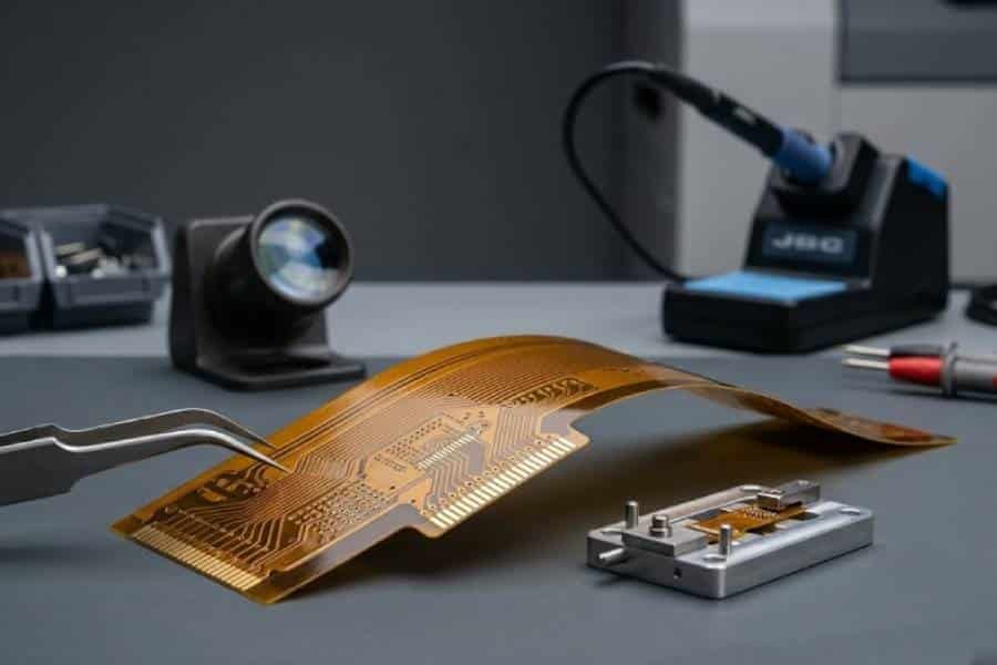
2. Use Proper Bend Radius
The bend radius should never be treated as an afterthought. A radius that is too tight can create concentrated strain in the copper and dielectric layers, which eventually leads to failure even if the board passes initial testing.
Different sources give different design targets depending on layer count and construction, but they all point to the same principle: the bend radius must be sized according to the board thickness and intended flex cycles. For long-term reliability, the safest approach is to build in margin rather than designing to the absolute minimum.
3. Add Strain Relief Where Needed
Strain relief is critical at transition points, connector edges, and stiffener boundaries. Without it, stress tends to concentrate exactly where the board changes from rigid to flexible, which is one of the most common failure locations in flex designs.
Rounded support edges, careful stiffener placement, and smooth transition geometry all help reduce tension risers. In practice, this means the flex section should never be forced to absorb sudden force from clamps, brackets, or enclosure edges.
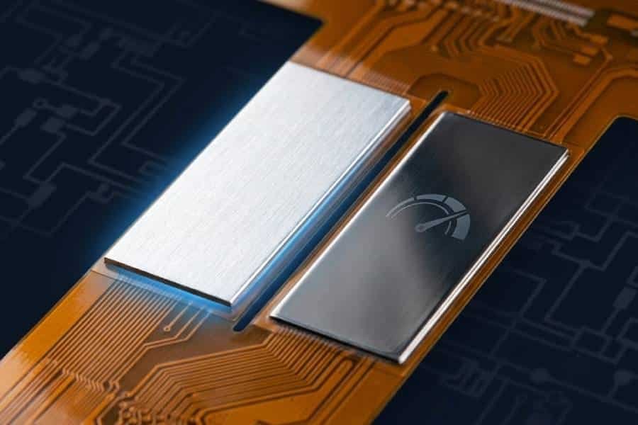
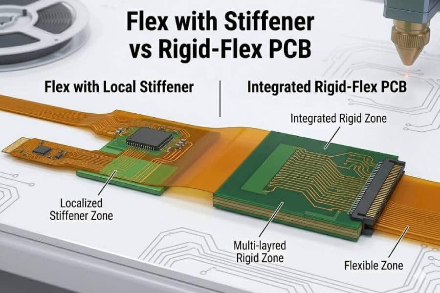
4. Match Stiffeners to the Application
Stiffeners are not used to make the whole board rigid; they are used only where local mechanical support is needed. Typical applications include connector areas, SMT mounting zones, and other locations where parts need a flatter and stronger surface during assembly or service.
It is also important to size and place stiffeners carefully so they support the board without creating a new stress concentration at the edge. Well-designed support areas improve assembly stability while preserving the flexibility of the rest of the circuit.
5. Prepare for Assembly Early
Flexible PCBs often need to be fixed in a fixture before reflow or pick-and-place so they stay flat during processing. Industry guidance describes fixation as a key step because flex boards can deform more easily than rigid boards during assembly.
Pre-baking is another important precaution, especially when the parts have been stored for a while or will go through heat exposure during soldering. Multiple flex-assembly references stress that moisture control helps reduce delamination, warping, and other heat-related defects.
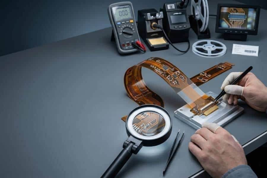
6. Handle the Board Gently
Even a well-designed flex PCB can fail if it is handled roughly. Pulling on the flex section, folding it too sharply, or placing it under mechanical tension during transport can damage the circuit before final installation even begins.
The safest practice is to hold the board in areas that are meant for support, avoid touching active bend zones, and keep the assembly protected until it is ready for installation. For flex circuits, handling discipline is part of reliability, not just packaging convenience.
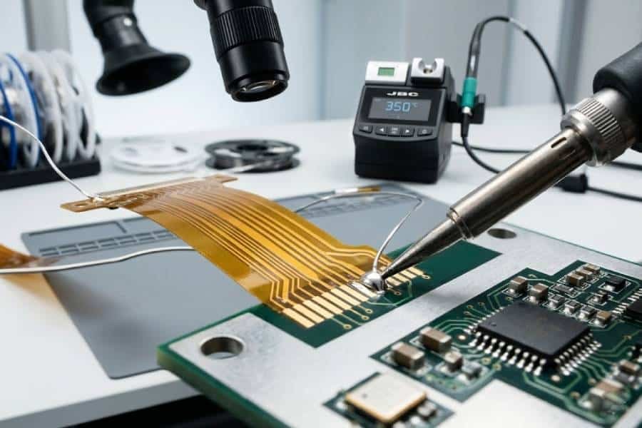
SMT and Soldering Precautions
SMT assembly is one of the most sensitive stages in flexible PCB manufacturing because the board must stay flat, stable, and dry while components are placed and soldered. If the flex circuit shifts during pick-and-place or deforms in reflow, the result can be misalignment, weak joints, or even layer damage.
The safest process is to treat fixture support, moisture control, and temperature profiling as mandatory steps rather than optional ones. Flex PCB assembly references consistently recommend pre-baking before soldering, fixing the board in a carrier or fixture, and using a controlled thermal profile to reduce warpage and delamination risk.
1. Fix the Board Before Reflow
A flex board should not enter reflow as a loose, unsupported sheet. Carrier fixtures or pallets help keep the board planar so components do not shift and the flex section does not move under heat.
This is especially important for thin flex circuits, because even slight vibration or sagging can affect solder paste alignment and joint quality. In practice, the fixture is part of the assembly process, not just a convenience tool.
2. Pre-Bake to Remove Moisture
Flexible materials can absorb moisture, and that moisture becomes a serious risk when the board goes through soldering heat. Pre-baking is widely recommended before all major soldering methods, including reflow and hand soldering, because it helps prevent delamination, blistering, and other heat-related defects.
The exact bake profile depends on material thickness and structure, but the key idea is simple: the board should be dry before soldering begins, and it should not sit too long in ambient air after baking. Good process control here can make a major difference in final reliability.
3. Control the Reflow Profile
Flex circuits generally need a gentler thermal profile than rigid boards. A smooth ramp-up, controlled peak temperature, and even cooling help reduce thermal shock and lower the chance of warpage or cracking.
Some process references also note that both time and temperature may need adjustment for flex boards, especially for thicker constructions or rigid-flex assemblies. The main objective is to achieve proper solder flow without stressing the substrate.
4. Protect Sensitive Areas During Heating
Areas near bends, stiffeners, and transition zones are more vulnerable during reflow because heat and mechanical stress can combine there. If solder pads are placed too close to bend regions, the board becomes more likely to fail later under movement or vibration.
That is why good flex assembly planning keeps critical joints away from high-stress zones whenever possible. When this is not possible, the design should compensate with reinforcement, proper pad placement, and a more conservative thermal process.
5. Minimize Rework Stress
Rework on flexible boards should be handled carefully because repeated heating can compound moisture and deformation risks. Even if the original assembly went well, aggressive rework can still damage pads, weaken adhesive bonds, or distort the circuit.
The safest approach is to keep rework localized, controlled, and as short as possible. If the board has already been pre-baked and then sits too long before rework, it may need to be baked again to maintain process stability.
6. Inspect After Soldering
Post-solder inspection is especially important for flex circuits because some defects are not obvious at first glance. Small warpage, partial delamination, or marginal solder joints may only appear after the board cools down or is mechanically flexed.
A good inspection step should check both electrical quality and physical condition. In flexible PCB assembly, reliability is not confirmed until the board has passed visual, structural, and functional review.
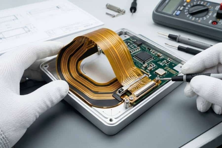
Installation and Mechanical Handling
Once the board has passed assembly, the installation stage still needs careful control because many flex failures happen after soldering, not during it. The main risks are over-bending, twisting, connector stress, and damage from enclosure edges or vibration.
A flexible PCB should always be routed and mounted according to its intended bend path. In practice, that means protecting the flex section from sharp folds, avoiding unnecessary movement, and making sure the board is secured so it cannot shift under load.
1. Do Not Exceed the Bend Limit
The most basic installation rule is to avoid over-flexing the circuit. If the installed shape forces the board tighter than its designed bend radius, the copper and dielectric layers can fatigue over time and eventually crack.
This matters even more for assemblies that flex repeatedly or operate in high-vibration environments. A conservative bend path is usually more reliable than forcing the flex to fit into a smaller space.
2. Secure the Board Properly
A flex circuit should be mounted so that the supported areas carry the load, while the active flex zone remains free to move as intended. Mounting hardware, adhesive support, and proper routing can all help reduce unwanted motion and prevent stress from concentrating near solder joints or connectors.
If the board is left partially loose, vibration and repeated motion can slowly damage the copper or break the connection at transition points. That is why secure mounting is not just a mechanical detail; it is a reliability requirement.
3. Protect Connectors and Interfaces
Connector regions are some of the most failure-prone areas in flex assemblies. If cable routing, insertion force, or enclosure alignment pulls on the flex tail, the connector can experience stress that eventually leads to intermittent contact or pad damage.
To reduce this risk, the flex tail should enter the connector without side loading, and the surrounding structure should leave enough room for a clean, controlled path. Good connector support also reduces the chance of damage during service or repeated mating cycles.
4. Avoid Sharp Edges and Abrasion
Enclosure edges, brackets, and metal cutouts can wear through a flex circuit if the board rubs against them during use. Even if the damage is not immediate, repeated contact can weaken the coverlay and expose the conductors later.
For that reason, installation should include a final check for clearance around all moving or contacting parts. If there is any chance of abrasion, the design should use extra protection, a better routing path, or a more secure mounting method.
5. Manage Vibration and Repeated Motion
In products exposed to vibration, the flex PCB must be treated as a dynamic mechanical part, not only an electrical interconnect. Long unsupported sections, weak fixation near connectors, and poor strain relief are common contributors to vibration-related failures.
A better approach is to shorten unsupported spans, reinforce the transition zones, and verify that the flex path will still be stable after repeated movement. This is especially important in industrial, automotive, and compact consumer products where reliability depends on long-term mechanical stability.
6. Confirm Final Fit Before Release
Before final release, the assembly should be checked in its actual installed position rather than only in the flat state. A board that looks perfect on the bench may still fail once it is folded, clamped, or inserted into the housing.
This final fit check should confirm bend direction, connector alignment, clearance, and stress points. In flex PCB work, the installed condition is the real condition, so the last inspection must reflect how the product will actually be used.
Common Failure Modes
Even when a flexible PCB is well designed and properly assembled, the wrong bend path, mounting method, or operating environment can still create failure over time. The most common problems are copper cracking, delamination, lifted pads, solder joint fatigue, and intermittent electrical opens.
The reason these failures happen is usually the same: mechanical stress is concentrated into a small area for too long. Once that stress repeats through vibration, motion, or thermal cycling, the circuit begins to degrade even if it looked fine at first.
1. Copper Cracking
Copper cracking is one of the most common flex failure modes because repeated bending gradually fatigues the conductor. If the bend radius is too tight, or if traces are routed through a stressed zone, the copper can stretch and eventually fracture.
To prevent this, the design should keep copper away from the most aggressive bend areas and avoid forcing the board into an unrealistic mechanical shape. Using proper bend rules and maintaining enough clearance around transition zones greatly improves conductor life.
2. Delamination
Delamination happens when layers begin to separate, often because of moisture, heat, or repeated mechanical stress. In flex circuits, this can appear after reflow, during vibration testing, or after long-term field use if the material stack is not well matched.
The best prevention method is a combination of material selection, pre-bake before assembly, and controlled mechanical loading during use. If the board is designed with proper bend limits and stable reinforcement, the layer interfaces are much less likely to fail.
3. Lifted Pads and Solder Joints
Lifted pads and solder joint failures often occur when the flex section transfers stress into the component area. This is especially common when components are too close to bend lines or when the board is allowed to move after assembly.
The most effective protection is to keep components in stiffened areas and use strain relief so the solder joint is not doing the job of mechanical support. That separation between electrical function and mechanical load is one of the most important reliability principles in flex design.
4. Intermittent Opens
Intermittent opens are particularly dangerous because they can hide during bench testing and only appear in real use. They usually happen when copper fatigue, connector stress, or micro-cracks create a connection that works only part of the time.
Because these faults are difficult to trace, the best strategy is prevention through design discipline: proper bend radius, controlled installation, and reinforced stress points. Once intermittent failures appear, the root cause is often mechanical rather than purely electrical.
5. How to Prevent These Failures
The easiest way to reduce flex PCB failures is to think of the board as a mechanical structure first and an electrical circuit second. That means defining bend zones early, avoiding vias and pads in stressed regions, and matching the material stack to the actual application environment.
It also means involving manufacturing and assembly early, because many problems can be avoided before fabrication starts. Early DFM review, proper strain relief, and realistic installation planning are usually far cheaper than repairing failures after release.
Best Practices Summary
The most reliable flexible PCB assemblies start with the same core principles: design the bend path carefully, keep stress away from sensitive areas, and treat assembly and installation as part of the mechanical design. When those basics are followed, the board is much more likely to survive both production and real-world use.
A good flex workflow also depends on early DFM review. That step helps catch bend-radius issues, poor component placement, and unsupported transition zones before fabrication, which is far cheaper than fixing failures later.
1. Design for the Actual Motion
A flex PCB should be designed around the exact motion it will experience in service. If the circuit bends only once during installation, the design targets are different from a board that flexes repeatedly in operation.
This is why bend radius, bend direction, and conductor placement all matter so much. The more accurately the design matches the real use case, the lower the stress on the copper and dielectric layers.
2. Reinforce Only Where Needed
Stiffeners, strain relief, and support layers should be used strategically rather than everywhere. The goal is to strengthen connector areas and assembly zones without reducing flexibility in the rest of the circuit.
This balance is one of the defining differences between a reliable flex design and one that only works on paper. A board that is too rigid in the wrong place can create new stress points, while a board with no reinforcement can fail during handling or installation.
3. Protect the Board Through Assembly
During SMT and soldering, the board should be fixed, dry, and thermally controlled so it does not shift or deform. Pre-baking, carrier support, and a controlled reflow profile are standard precautions for keeping flex assemblies stable.
These process controls are not optional details. They directly affect solder quality, layer integrity, and the long-term reliability of the finished assembly.
4. Install With Mechanical Discipline
After assembly, the flex circuit still needs protection from over-bending, vibration, sharp edges, and connector strain. Secure mounting and a clean bend path are essential to prevent damage that may only show up after deployment.
In other words, a flexible PCB is only reliable if the final enclosure and installation method respect its mechanical limits. If the product forces the board into a tighter or harsher shape than intended, the design margin disappears quickly.
5. Review Failures Early
The most useful habit in flex PCB work is to identify failure risks before they become field failures. Cracked copper, delamination, lifted pads, and intermittent opens are often preventable if the design is reviewed from both electrical and mechanical perspectives at the start.
That is why early collaboration with the manufacturer is so valuable. A practical DFM review can usually catch the weak points in bend zones, support zones, and connector areas before production begins.
FAQ
The most important precaution is to control mechanical stress, especially in bend zones, connector areas, and transition points. Proper bend radius, strain relief, and fixture support are central to reliable flex assembly.
Yes. Flexible PCB materials can absorb moisture, so pre-baking before soldering is widely recommended to reduce delamination, warpage, and reflow-related damage.
Stiffeners are used to reinforce areas that need support, such as connectors or component mounting zones, while leaving the rest of the circuit flexible.
Common causes include over-bending, vibration, connector stress, sharp enclosure edges, and repeated motion that exceeds the circuit’s mechanical design limits.
The best approach is to run an early DFM review, define the bend path clearly, keep pads and vias out of high-stress areas, and confirm the assembly plan before fabrication.
Conclusion
Flexible PCB assembly and installation require careful planning because the board must survive not only soldering, but also bending, mounting, vibration, and long-term mechanical stress. The most reliable results come from combining good design rules, controlled assembly, and disciplined installation practices.
If you want a flex circuit to perform consistently, the key is simple: protect the bend area, reinforce the stress points, control moisture and heat during assembly, and make sure the final installation respects the board’s mechanical limits.
If you are planning a flexible PCB project, it is worth reviewing the design and assembly process early so potential failure points can be eliminated before production. Our team can support flexible PCB assembly, design review, and manufacturability checks to help improve reliability from the start.