Table of Contents
Flexible PCB stackup is one of the most important decisions in flex circuit design. It affects bend life, signal integrity, and whether the board can be manufactured reliably at scale
Why Flexible PCB Stackup Matters
A good stackup does more than define the layer count. It helps control mechanical stress, keeps traces stable during bending, and reduces the risk of warpage, cracks, and assembly problems.
For flex and rigid-flex boards, the stackup also shapes how the circuit behaves in real use. Materials, copper thickness, coverlay, and stiffeners all work together, so a poor choice in one area can affect both performance and yield.
That is why stackup planning should start early, before layout is finalized. A clear stackup drawing and DFM review help the fabricator understand the construction and avoid costly back-and-forth later.
Key Elements of a Flexible PCB Stackup
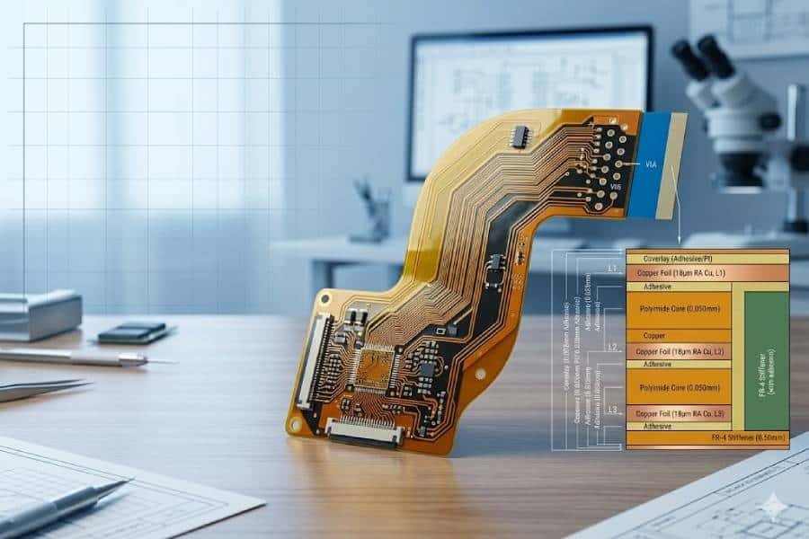
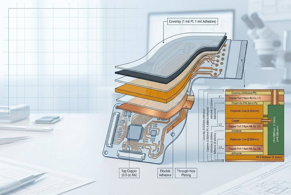
A flexible PCB stackup is built from a few core elements: copper, dielectric material, adhesive, coverlay, and stiffeners. Each one affects how the board bends, how it is protected, and how it will perform during fabrication and assembly.
The flexible section is usually based on polyimide for its thermal stability and mechanical flexibility, while copper thickness and adhesive selection must match the bending requirement. Coverlay is typically used to insulate and protect the flex area, and stiffeners are added where connectors or components need extra support.
In practice, the best stackup is the one that balances flexibility, durability, and manufacturability. That is why material selection should be defined together with the fabricator, especially for rigid-flex designs or boards with tight bend requirements.
Base Materials and Copper Options
The base material in a flexible PCB stackup is usually polyimide because it offers a strong balance of thermal stability, chemical resistance, and mechanical flexibility. In rigid-flex designs, FR4 or polyimide laminates may also be used in the rigid sections to provide structural support where components, connectors, and plated holes must remain stable.
Copper selection is just as important as the dielectric choice. Rolled annealed copper is often preferred in flex areas because it is more ductile and performs better under repeated bending, while electro-deposited copper may be more suitable in rigid sections or cost-sensitive constructions. In general, the heavier the copper and the thicker the core, the less flexible the circuit becomes, so these choices should always match the actual bending requirement.
Coverlay, Adhesive, and Protection Layers
Coverlay is the standard protective layer used in many flex circuits because it insulates and seals the outer copper while preserving flexibility. It is typically made from polyimide film with adhesive, and the combination of film thickness and adhesive thickness should be chosen according to the design’s reliability, bend, and manufacturing needs.
Adhesives do more than bond materials together. They are also used in coverlay lamination, stiffener attachment, and other stackup interfaces, so the adhesive system can affect thickness, flexibility, thermal resistance, and long-term durability. In some designs, adhesiveless constructions are preferred because removing the acrylic adhesive layer can reduce thickness and improve thermal stability in the flex section.
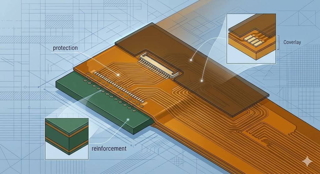
Stiffeners and Transition Zones
Stiffeners are added to selected areas of a flex circuit to provide local reinforcement, especially under connectors, component pads, or handling zones. Common stiffener materials include FR4, polyimide, and sometimes metal, depending on the required thickness, rigidity, and assembly support.
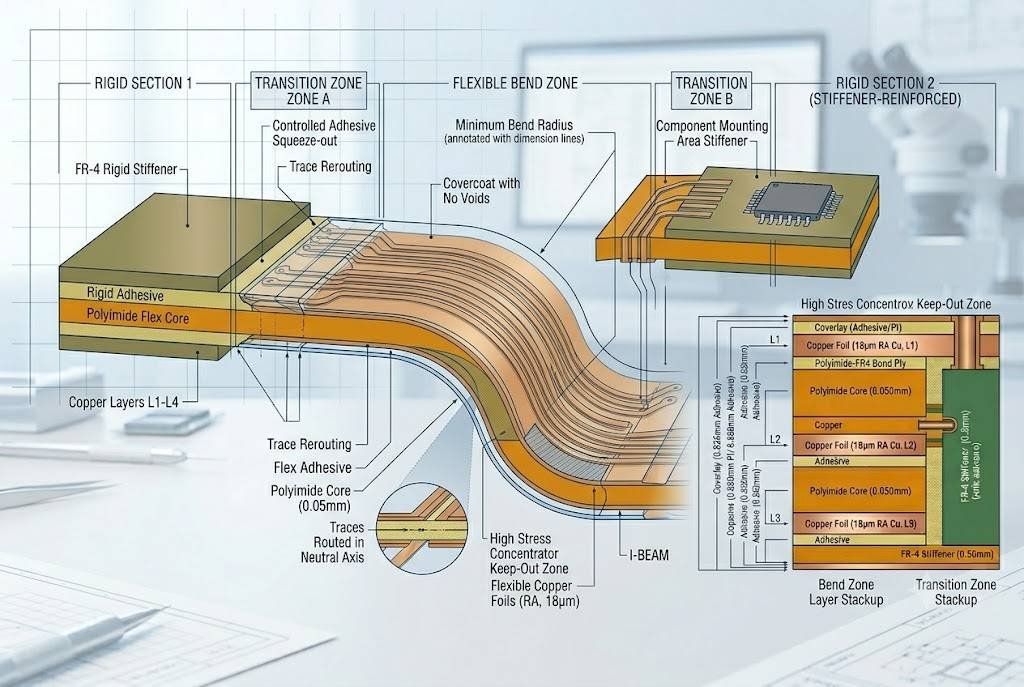
The transition between flexible sections, coverlay, and stiffened or rigid areas should be designed carefully because this is often where stress concentrates. Overlap, spacing, and geometry in these zones affect crack resistance, dimensional stability, and manufacturability, so the transition area should always be clearly defined in the stackup and fabrication drawing.
Stackup Optimization Rules for Reliable Flex Design
A flexible PCB stackup should be designed to support both electrical performance and mechanical durability. The goal is to keep the flex area thin, balanced, and free from unnecessary stress points.
A symmetrical stackup is usually the safest starting point, especially for rigid-flex boards or designs that must survive repeated bending. When the copper and dielectric layers are balanced, the board is less likely to warp, twist, or shift its neutral axis during use.
In bend regions, traces should be routed as smoothly as possible and kept away from the highest-stress areas. Vias, sharp corners, and abrupt layer changes should be minimized, while transition zones should be clearly defined so the fabricator can build the board without guesswork.
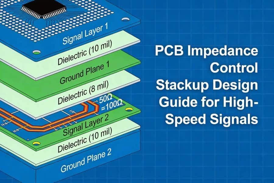
Where impedance control is required, the stackup should preserve a stable reference path without making the flex section too stiff. For some designs, a hatched ground plane can help reduce copper coverage and improve flexibility, but the exact approach should always match the application and manufacturability requirements.
Keep the Stackup Symmetric
A symmetric stackup helps keep mechanical stress balanced across the structure. When copper, dielectric, and bonding layers are arranged evenly, the board is less likely to warp during lamination or shift its neutral axis during bending.
This is especially important in rigid-flex designs, where mismatched constructions can create uneven stress between rigid and flexible sections. Even when perfect symmetry is not possible, designers should still aim to keep the flex area as balanced and predictable as possible.
Control Bend Radius and Thickness
Bend radius should always be defined according to the actual stackup, not treated as a generic rule. Layer count, copper thickness, adhesive thickness, and whether the bend is static or dynamic all influence how tightly the circuit can bend without damage.
In most cases, a thinner flex section gives better bend performance and longer dynamic life. If the design requires more layers or added reinforcement, the bend area should be planned carefully so the structure does not become too stiff for the intended application.
Route Traces Carefully in Flex Areas
Trace routing in flex areas should reduce stress concentration as much as possible. Smooth curves are preferred over sharp angles, and traces should be arranged to support bending rather than resist it.
Vias, plated holes, and large exposed copper features should be kept out of bend zones whenever possible. In multilayer flex regions, staggered routing and careful spacing can also help reduce local stiffness and improve long-term reliability.
Handle Transition Zones and Reference Planes Properly
The rigid-to-flex transition zone is one of the most sensitive parts of the design because both mechanical and electrical conditions change there. Clear boundaries, proper keep-out spacing, and gradual geometric transitions help reduce crack risk and improve manufacturability.
For high-speed or impedance-controlled designs, reference planes should support signal return without making the flex section unnecessarily rigid. In some cases, a hatched ground plane is used to balance flexibility and electrical performance, but the exact structure should be chosen according to the signal requirements and the manufacturer’s process capability.
How Stackup Choices Affect Manufacturing and Assembly
Stackup decisions do not stop at electrical performance. They also affect how the board will be laminated, drilled, assembled, and inspected during production.
A stackup that is too thick or too complex can make fabrication harder and reduce process stability. In flex and rigid-flex designs, material choice, bonding method, and layer balance all influence whether the board will stay flat, align properly, and survive the manufacturing process without defects.
Assembly also depends on the stackup. Areas with stiffeners, connector pads, and component mounts must be planned early so the fabricator and assembler can handle support, registration, and soldering correctly.
That is why DFM review is so important for flexible PCB projects. When the stackup is shared early, the manufacturer can confirm material availability, construction limits, and any changes needed before production begins.
Lamination and Material Selection
Lamination quality depends heavily on how the stackup is built and how well the selected materials work together. Substrate type, adhesive system, copper thickness, and reinforcement details all affect thermal behavior, dimensional stability, and the overall consistency of the fabrication process.
For this reason, material selection should always reflect the actual application rather than a default construction. Static and dynamic flex designs often require different thickness targets, bonding methods, and reinforcement strategies, so early coordination with the manufacturer helps reduce risk before tooling begins.
Registration and Alignment Control
Registration becomes more challenging as the stackup grows more complex, especially in rigid-flex constructions with multiple bonded sections. During fabrication, the alignment of copper layers, coverlay openings, stiffeners, and drilled features must remain tightly controlled to avoid dimensional mismatch and assembly problems.
This is one reason why clear fabrication drawings matter so much. Alignment holes, coverlay tolerances, stiffener clearances, and layer-to-layer registration notes should be defined early so the manufacturer can build the design without making assumptions.
Testing, Assembly, and DFM Review
Testing and assembly performance are closely tied to stackup quality. If thickness, transition zones, coverlay openings, and stiffener placement are not planned correctly, the board may become harder to solder, fixture, inspect, or verify during production.
A thorough DFM review helps catch these issues before fabrication starts. It allows the manufacturer to evaluate bend-zone design, stackup balance, material compatibility, assembly constraints, and inspection requirements, which reduces rework, shortens iteration cycles, and improves first-pass yield.
Common Stackup Mistakes to Avoid
One of the most common mistakes is making the flex section too thick or too complex. Extra copper, heavy adhesive, or unnecessary layers can reduce bend life and make the board harder to manufacture reliably.
Another frequent problem is poor placement of vias, pads, or stiffener edges near the bend zone. These features create stress concentration, which can lead to cracking, delamination, or copper fatigue over time.
Designers also sometimes forget to define the rigid-to-flex transition clearly. If the stackup drawing does not show the transition zone, keep-out areas, and reinforcement details, the fabricator may have to make assumptions that increase risk during production.
Finally, it is a mistake to treat stackup as a last-minute note instead of a core design input. Early DFM review helps confirm material availability, construction limits, and mechanical constraints before the project moves into fabrication.
FAQ
The ideal stackup depends on whether the circuit is static or dynamic, how many bends it must survive, and whether impedance control is required. In general, a thinner and more symmetrical construction is easier to bend and manufacture reliably.
Yes, symmetry is usually recommended because it helps reduce warpage and mechanical imbalance during lamination and bending. This is especially important for rigid-flex boards and multilayer flex designs.
Coverlay is the common protective layer used in flexible sections because it remains flexible and protects the copper traces. Solder mask is typically used only in stiffened or rigid areas where flexibility is not needed.
Stiffeners are usually added in connector zones, component mounting areas, or other locations that need extra support. They should not be placed in bend areas because they increase stiffness and can raise mechanical stress.
It is generally best to avoid vias in bend areas because they can create stress concentration and lead to cracking or fatigue. If a design absolutely requires them, the manufacturer should review the construction very carefully.
DFM review helps confirm that the chosen materials, thickness, and transition zones can actually be built without defects. It also reduces the risk of late design changes, yield loss, and assembly problems.
If you are planning a flexible PCB or rigid-flex project, the stackup should be reviewed before layout is finalized. A clear early stackup can improve reliability, simplify fabrication, and reduce the risk of costly revisions.