Table of Contents
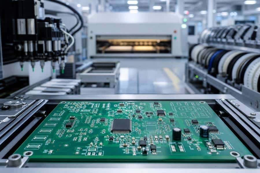
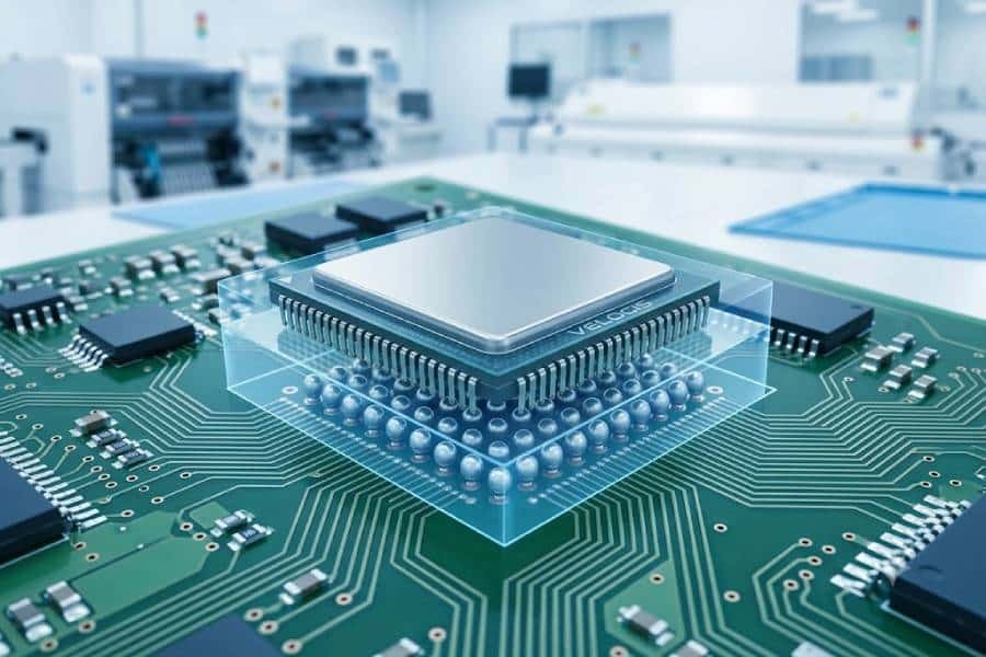
In today’s competitive electronics industry, even the smallest defect in a PCB assembly can lead to product failures, costly rework, or damaged reputation. As a full-service PCB manufacturer and assembly provider, we at JHYPCB know that reliable quality control is the foundation of every successful project. Two of the most critical automated inspection technologies in modern SMT lines — SPI (Solder Paste Inspection) and AOI (Automated Optical Inspection) — play complementary but distinctly important roles in catching issues before they become expensive problems.
While both systems use advanced imaging to improve quality, they inspect completely different stages of the assembly process. Understanding the key differences between AOI and SPI helps engineers and procurement teams make better decisions when choosing a manufacturing partner. In this guide, we’ll explore how each technology works, where they differ, and why leading PCB assembly services like ours rely on both to deliver consistently high-quality boards.
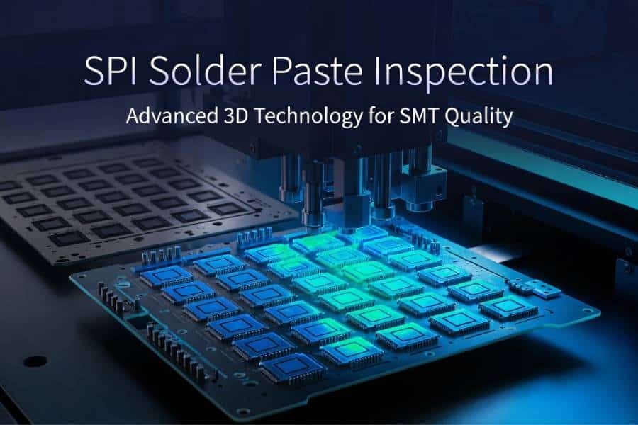
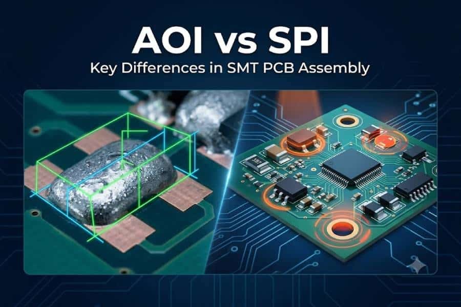
What Is SPI (Solder Paste Inspection)?
SPI stands for Solder Paste Inspection. As the name suggests, it focuses on the very first critical step in the SMT process: solder paste printing.
After the solder paste is applied to the bare PCB through a stencil, an SPI system uses 3D imaging technology to measure key parameters such as:
- Paste volume
- Paste height (thickness)
- Paste area
- Alignment and position
Why does this matter? Even tiny variations in solder paste can lead to major issues later — insufficient paste may cause open joints, while excess paste can create bridges or shorts. By catching these problems immediately after printing and before component placement, SPI acts as an early warning system that prevents defective boards from moving further down the line.
In high-density PCB designs common in modern electronics, SPI has become especially valuable. It helps maintain consistency across thousands of pads, reducing rework and improving first-pass yield.
What Is AOI (Automated Optical Inspection)?
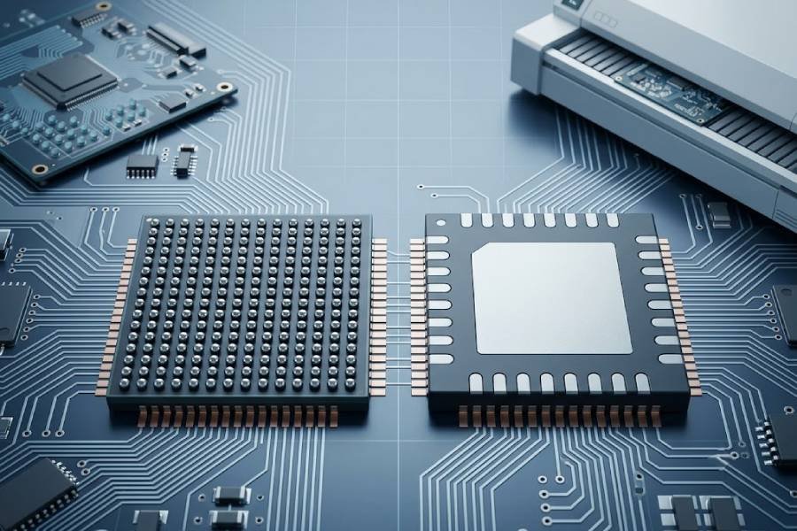
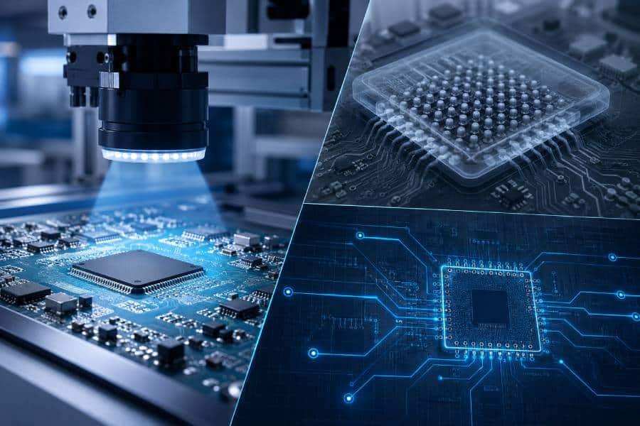
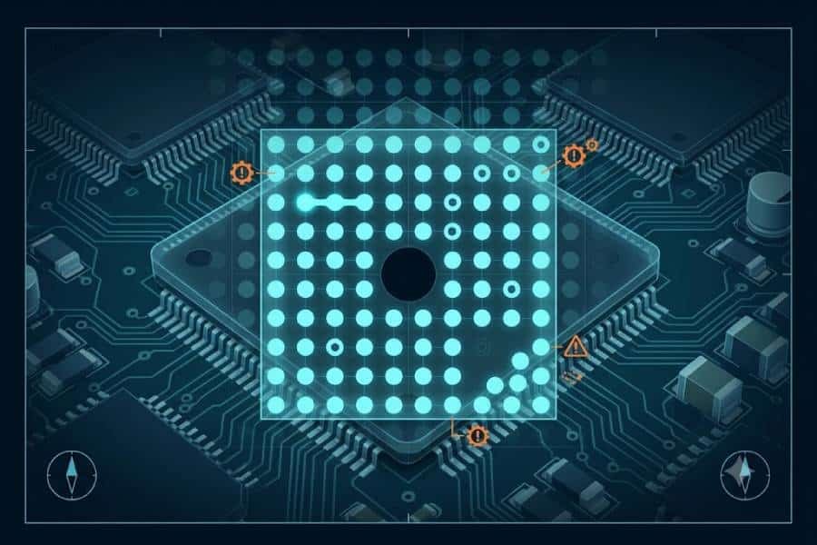
AOI, or Automated Optical Inspection, comes into play after components have been placed and soldered. It uses high-resolution cameras and advanced algorithms to visually inspect the assembled board for a wide range of defects, including:
- Missing or misplaced components
- Wrong component orientation or polarity
- Solder joint quality (bridges, insufficient solder, cold joints)
- Tombstoning, lifted leads, or skewing
AOI systems can be deployed at multiple stages: after pick-and-place (pre-reflow) or after reflow soldering (post-reflow). Post-reflow AOI is particularly powerful because it verifies the final assembly quality before the board moves to functional testing or shipping.
Unlike manual visual inspection, AOI is fast, repeatable, and capable of detecting microscopic issues that even experienced operators might miss under fatigue.
Core Differences Between AOI and SPI in SMT Assembly
While both SPI and AOI are essential automated optical inspection tools, they serve distinct purposes in the SMT process. Here’s a clear comparison:
| Aspect | SPI (Solder Paste Inspection) | AOI (Automated Optical Inspection) |
|---|---|---|
| Inspection Stage | After solder paste printing, before placement | After component placement and/or reflow soldering |
| Primary Target | Solder paste deposits | Components, solder joints, and board appearance |
| Main Defects Detected | Volume, height, area, alignment issues | Missing parts, misalignment, polarity errors, solder defects |
| Technology | Primarily 3D laser or structured light | 2D/3D cameras with AI-enhanced vision |
| Role in Production | Process control & prevention | Quality verification & final assurance |
| Typical Benefit | Reduces defects entering the line | Ensures final product meets specifications |
This table highlights a fundamental truth in PCB assembly: SPI and AOI are not competitors — they are complementary.
How SPI and AOI Work Together in a Real Production Line
Imagine a complete SMT line at JHYPCB. The process flows like this:
- Solder paste is printed.
- SPI immediately checks the paste quality. If issues are found, the stencil can be cleaned or the board reprinted before components are placed — saving significant time and material.
- Components are placed by high-speed pick-and-place machines.
- AOI (pre-reflow) can optionally verify placement.
- The board goes through reflow soldering.
- Post-reflow AOI performs a final visual check of the assembled board.
This layered approach creates multiple quality gates. In our experience manufacturing complex multilayer and rigid-flex PCBs, combining SPI and AOI typically results in significantly higher first-pass yields and lower defect rates compared to using either technology alone.
When Should You Use SPI, AOI, or Both?
Use SPI when:
- Your design has fine-pitch components or high-density layouts
- Solder paste consistency is critical (e.g., automotive, medical, or aerospace applications)
- You want to optimize the printing process and reduce downstream rework
Use AOI when:
- You need to verify component placement and final solder joint quality
- Your products require strict traceability and documentation
- You’re performing final quality assurance before shipment
Use Both (Recommended): For most professional PCB assembly projects today, the answer is both. Leading manufacturers like JHYPCB integrate SPI and AOI as standard practice in our turnkey PCB assembly services. This combination is especially important for clients working on prototypes that will later scale to volume production.
Common Misconceptions About SPI and AOI
One frequent misunderstanding is thinking that one technology can fully replace the other. In reality, SPI cannot detect component placement or solder joint issues, while AOI cannot accurately assess paste volume before reflow. They solve different problems at different stages.
Another misconception is that automated inspection makes human oversight unnecessary. The truth is that experienced engineers still review results, set up inspection programs, and make final judgments — especially on complex rigid-flex or mixed-technology assemblies.
Benefits for Your PCB Projects at JHYPCB
By implementing both SPI and AOI in our SMT lines, JHYPCB delivers measurable advantages to our clients:
- Higher reliability and consistency across prototypes, small batches, and mass production
- Faster identification and correction of process issues
- Reduced overall manufacturing costs through lower rework rates
- Full documentation and traceability for quality-sensitive industries
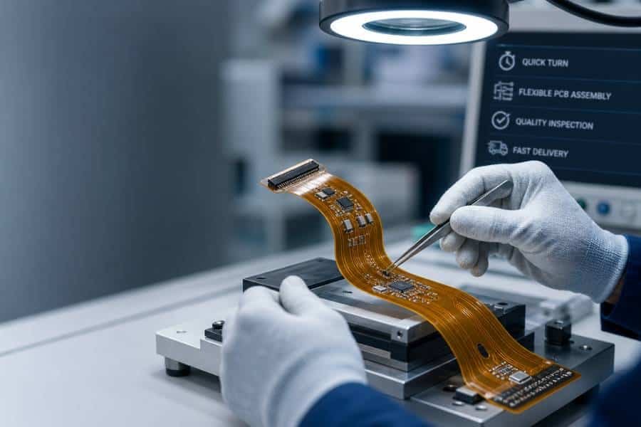
Whether you need single-sided PCB manufacturing, advanced multilayer rigid-flex boards, or complete turnkey PCB assembly including component sourcing and SMT stencil production, our inspection capabilities help ensure your products meet the highest standards.
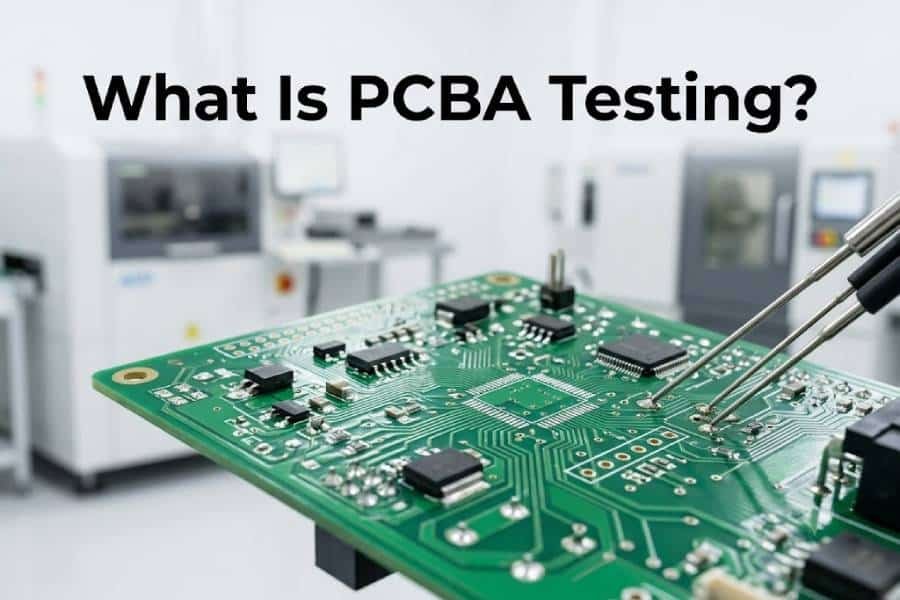
Conclusion
Understanding the difference between AOI and SPI is key to appreciating the sophistication behind modern SMT PCB assembly. SPI protects your process at the beginning by ensuring perfect solder paste deposition, while AOI verifies the final assembly quality. Together, they form a robust quality control system that minimizes defects and maximizes confidence in every board.
At JHYPCB, we don’t just manufacture PCBs — we deliver peace of mind through expert engineering, advanced inspection technologies, and customer-focused service. If you have an upcoming project or questions about how SPI, AOI, and other inspection methods can benefit your product, our team is ready to help.
Contact us today at sales@pcbjhy.com to discuss your PCB manufacturing and assembly needs. Let’s build reliable electronics together.
FAQ
SPI inspects solder paste after printing, while AOI inspects components and solder joints after placement and reflow. They target different stages and defect types in the SMT process.
No. SPI and AOI are complementary. Using both provides the most comprehensive quality control.
AOI primarily checks post-reflow results. SPI is the dedicated technology for paste inspection before components are placed.
Catching paste issues early prevents many downstream defects, saving time and cost. AOI then verifies the complete assembly.
It depends on your design and requirements. For most professional applications, the best choice is a partner like JHYPCB that uses both SPI and AOI as standard.