Table of Contents
In the world of electronics manufacturing, the difference between a reliable product and a field failure often comes down to the smallest details — like how evenly solder paste is applied to a PCB. Over the years at JHYPCB, we’ve seen firsthand how solder paste printing issues can cause headaches downstream: insufficient solder leading to weak joints, excess paste causing bridges, or misalignment resulting in open circuits. That’s exactly why Solder Paste Inspection (SPI) has become an indispensable part of our SMT lines. In this article, we’ll dive deep into SPI technology, its working principles, and how it helps us — and our customers — achieve higher yields and better reliability.
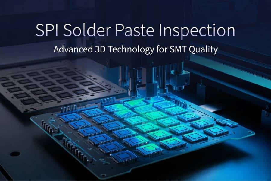
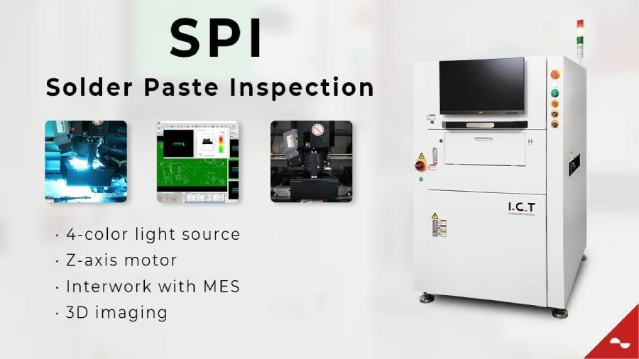
What is Solder Paste Inspection (SPI)?
Solder Paste Inspection (SPI) is an automated, non-contact optical inspection process that verifies the quality of solder paste deposits immediately after stencil printing and before component placement. It measures critical parameters such as paste volume, height, area, position, and shape with high precision.
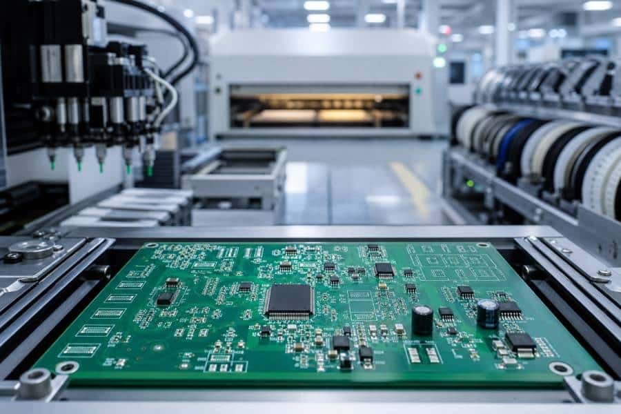
In a typical SMT process flow, SPI sits right between the solder paste printer and the pick-and-place machine. This strategic position allows manufacturers to catch and correct issues early — before components are placed and reflow soldering locks in any defects. At JHYPCB, we perform 100% SPI inspection on production boards to ensure consistent quality across prototypes, small batches, and high-volume runs.
How Does SPI Technology Work? (Especially 3D SPI)
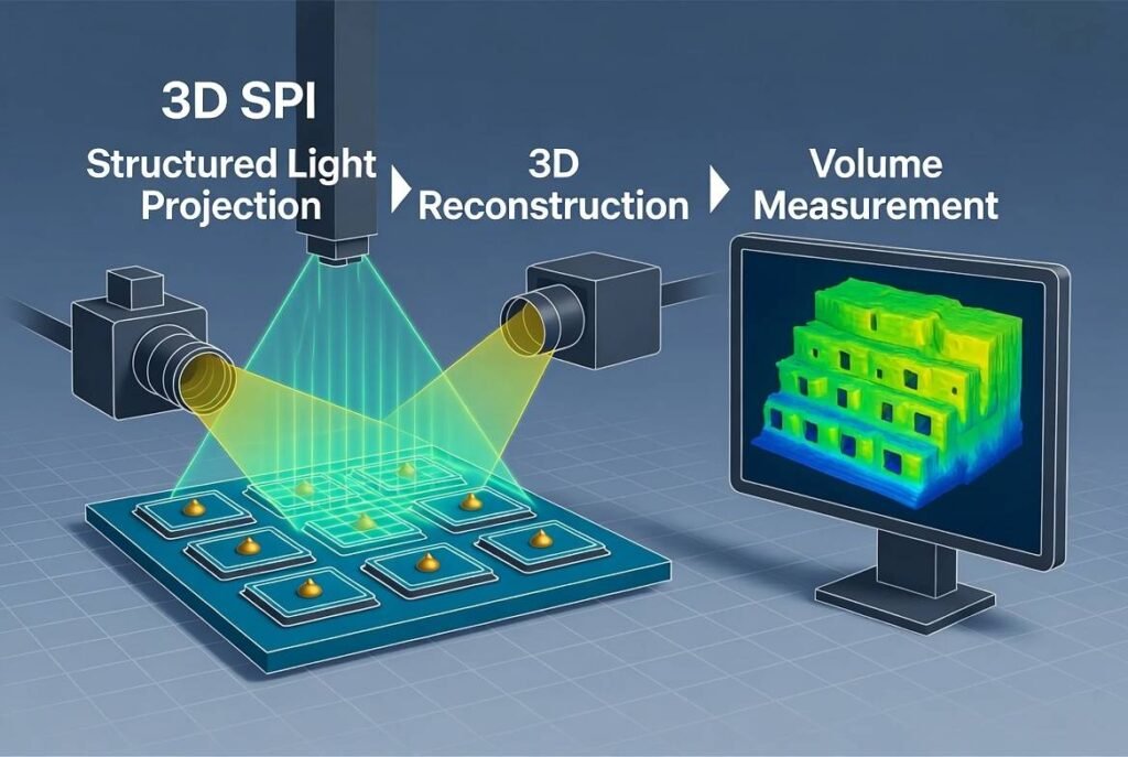
Modern SPI systems, particularly 3D SPI, go far beyond simple 2D imaging. Here’s how it works in practice:
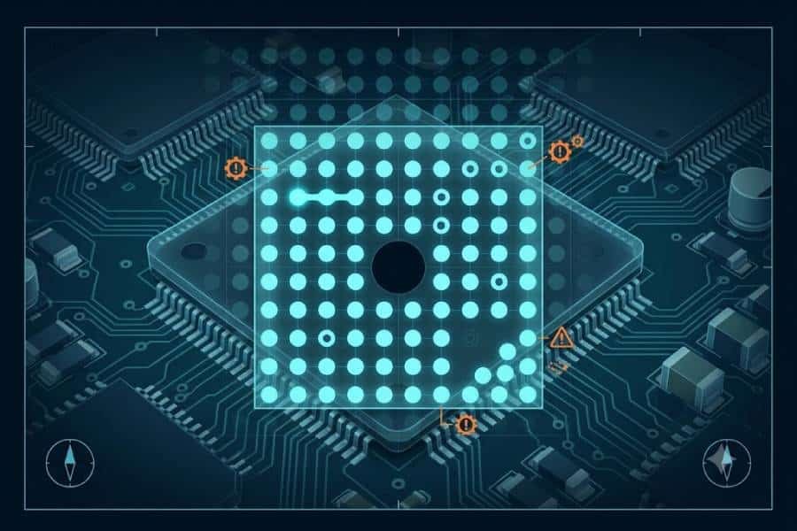
The system projects structured light (such as laser lines or fringe patterns) onto the PCB surface. High-resolution cameras capture the deformation of these patterns caused by the three-dimensional shape of the solder paste deposits. Using advanced algorithms like phase-shift profilometry or laser triangulation, the software reconstructs a precise 3D model of each paste deposit.
This model is then compared against the Gerber data and predefined acceptance criteria. For example, it can calculate the exact volume of paste on a fine-pitch pad (critical for components like 0.4mm QFNs or 01005 chips) and flag any deviation in height or coplanarity.
From our experience, 3D SPI provides measurements with sub-micrometer accuracy, which 2D systems simply cannot match. This level of detail is essential for today’s high-density, miniaturized designs.
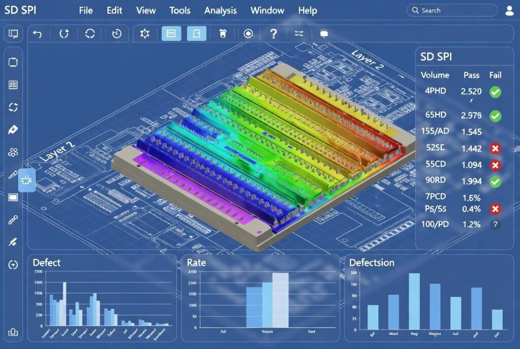
Common Defects Detected by SPI
SPI excels at identifying issues that are invisible to the naked eye or would only show up after reflow. Key defects include:
- Insufficient solder paste: Too little volume, leading to weak or open joints.
- Excess solder paste: Risk of bridging or solder balls.
- Misalignment/offset: Paste shifted from pad center due to stencil misalignment or printer issues.
- Bridging or slumping: Paste connecting adjacent pads or collapsing at the edges.
- Missing or incomplete deposits: Caused by stencil clogging or poor paste release.
- Peaking or dog-earing: Irregular shapes affecting wetting during reflow.
By catching these early, we prevent defects from propagating through the line, significantly reducing rework rates.
Key Advantages of Implementing SPI Technology
Beyond defect detection, SPI delivers measurable business benefits. In our production, we’ve observed:
- Higher first-pass yields: Early correction reduces defects by catching 60-80% of paste-related issues before they become costly problems.
- Closed-loop process control: SPI data feeds back to the printer in real time, automatically adjusting parameters like squeegee pressure, speed, or stencil cleaning frequency.
- Cost savings: Less rework, scrap, and manual inspection time translates directly to lower manufacturing costs.
- Improved long-term reliability: Consistent paste volume leads to stronger solder joints, which is vital for automotive, medical, and industrial applications.
- Data-driven continuous improvement: Trend analysis helps us optimize stencils, paste types, and printing parameters over time.
For high-mix or high-reliability projects, these advantages make SPI a smart investment rather than just an added step.
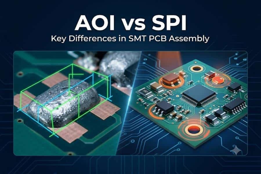
SPI vs AOI: Understanding the Differences
Many customers ask us about SPI versus Automated Optical Inspection (AOI). While both are essential, they serve different purposes:
- SPI focuses on the solder paste printing stage — checking volume, height, and position before components are placed.
- AOI inspects component placement and solder joints after placement or reflow, looking for missing parts, polarity issues, or joint quality.
They are complementary: SPI prevents paste problems, while AOI verifies the downstream results. At JHYPCB, we use both (plus X-ray when needed) as part of our comprehensive quality system.
SPI Equipment Selection Considerations
Choosing the right SPI system matters. Key factors we evaluate include:
- Inspection speed and accuracy — Must keep up with high-speed lines without compromising precision.
- True 3D capability — Essential for volume measurement on dense boards.
- Software intelligence — User-friendly interface, strong statistical process control (SPC), and easy integration with MES systems.
- Flexibility — Support for various PCB sizes, thicknesses, and component densities.
- Closed-loop readiness — Ability to communicate directly with printers for automatic corrections.
We recommend partnering with manufacturers who understand your specific production needs rather than buying the most expensive option.
Real-World Applications Across Industries
SPI technology shines in demanding sectors:
- Consumer electronics (smartphones, wearables) requiring ultra-fine pitch.
- Automotive and industrial controls needing high reliability under harsh conditions.
- Medical devices and communication equipment where zero defects are the goal.
In our turnkey PCB assembly projects, SPI helps us confidently handle everything from rigid PCBs and flexible circuits to complex rigid-flex designs.
Common Challenges with SPI and How to Overcome Them
No technology is perfect. Common issues include false calls due to paste variation, calibration drift, or suboptimal stencil design. Our solutions? Rigorous daily calibration, controlled paste handling (temperature and humidity), regular DFM reviews, and experienced process engineers who interpret data holistically rather than relying solely on machine pass/fail signals.
Conclusion: Elevating PCB Assembly Quality with SPI
Solder Paste Inspection (SPI), especially 3D SPI, has transformed how we approach quality in SMT PCB assembly. It’s not just about catching defects — it’s about building a more robust, efficient, and reliable manufacturing process from the very first step.
At JHYPCB, we combine advanced SPI technology with years of hands-on expertise in PCB manufacturing and assembly — including SMT, THT, mixed technology, turnkey solutions, component sourcing, and SMT stencils. Whether you need prototypes or volume production, we’re committed to delivering boards you can trust.
Have questions about SPI, your next PCB project, or how we can optimize your assembly process? Feel free to reach out to our team at sales@pcbjhy.com. We’d love to discuss how we can support your success.
FAQ
SPI inspects solder paste before component placement, while AOI checks components and joints after placement or reflow. They work together for comprehensive quality control.
By detecting paste issues early, SPI prevents many defects from reaching later stages, reducing rework and increasing first-pass success.
High-density boards with fine-pitch components, BGAs, and complex designs in automotive, medical, and industrial applications.
SPI greatly reduces the need for manual checks but works best combined with engineering oversight and other inspection methods for the highest confidence.