Table of Contents
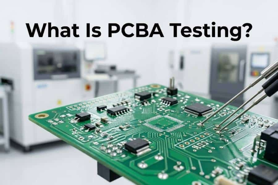
PCBA testing is the process of inspecting and verifying an assembled printed circuit board to make sure it has been built correctly and performs as intended. In practical terms, it is the checkpoint between assembly and shipment that helps manufacturers catch soldering defects, component errors, electrical faults, and functional problems before the board reaches the customer.
For both OEMs and PCB assembly suppliers, PCBA testing is not just a routine quality step. It is a critical part of risk control because it helps reduce rework, prevent field failures, and improve overall product reliability. Depending on the product type, package complexity, and production volume, the testing strategy may include AOI, X-ray inspection, ICT, flying probe, or functional testing.
If your team is comparing suppliers or preparing an RFQ, this topic also connects closely with the broader assembly workflow, including the main PCB assembly process steps, how to evaluate SMT PCB assembly quality: a buyer’s checklist, and how to get a quote and order PCB assembly.
What Is PCBA Testing?
PCBA testing refers to the inspection and electrical verification steps used to confirm that a completed circuit board assembly meets design intent and works correctly before delivery. Unlike bare PCB testing, which focuses on the fabricated board itself, PCBA testing takes place after components have been mounted and soldered, so it can identify real assembly-related faults.
These faults may include missing or rotated components, polarity errors, solder bridges, open circuits, weak joints, or hidden issues under advanced packages. Because of this, PCBA testing is not limited to one type of check. It usually combines optical inspection, electrical verification, and functional validation in order to build a more complete picture of board quality.
For readers who are still comparing terminology, it also helps to review PCB vs PCBA.
Why PCBA Testing Matters
A board can look acceptable after assembly and still fail in actual use. PCBA testing matters because many faults are not obvious from appearance alone, especially when the issue involves incorrect component values, hidden solder joints, intermittent opens, or unstable circuit behavior after power-up.
From a manufacturing perspective, testing helps catch problems before they turn into expensive rework, returns, or field failures. From a buyer’s perspective, it provides confidence that the delivered assemblies match the design requirements and can perform reliably in the final application.
This is also why many buyers review related quality content such as how to evaluate SMT PCB assembly quality: a buyer’s checklist, IPC standards in SMT PCB assembly: what you need to know, and common defects in lead-free PCB assembly and how to prevent them.
Common PCBA Test Methods
No single test method can detect every possible assembly problem. In practice, manufacturers choose a mix of test methods based on defect risk, package type, required coverage, and production stage.
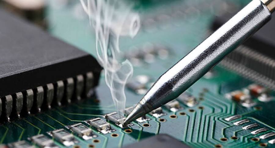
Visual Inspection
Visual inspection is the most basic quality screen and is often used to identify obvious issues such as missing parts, visible soldering defects, surface damage, or incorrect orientation. Although simple, it still plays a useful role as an early filter in both prototype and production workflows.
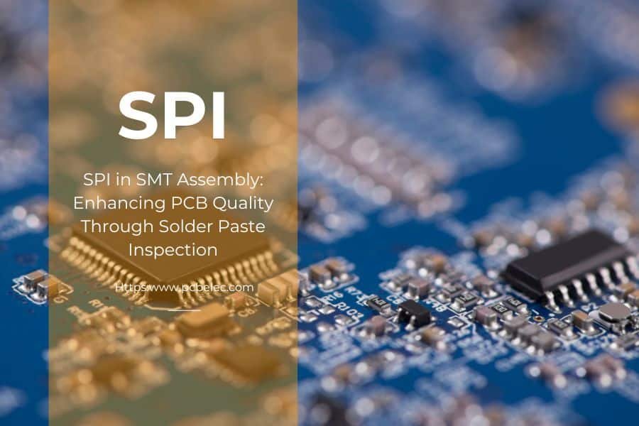
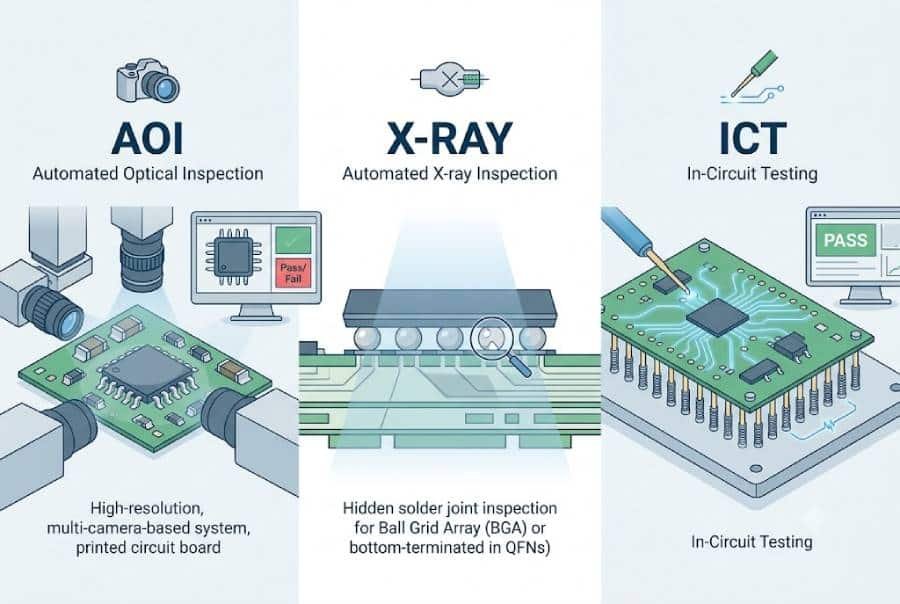
AOI
Automated Optical Inspection uses imaging systems and software to inspect component placement and visible solder joints after assembly. It is widely used in SMT lines because it can quickly detect many common surface-level defects with high consistency.
For a deeper look at this method, see AOI in SMT PCB assembly: how automated optical inspection improves PCB quality.
X-Ray Inspection
X-ray inspection is used when solder joints cannot be seen from the outside, especially with BGA, QFN, CSP, and other bottom-terminated packages. It is particularly valuable for detecting voids, hidden bridges, and internal solder-joint problems that AOI cannot confirm reliably.
This topic connects naturally with X-ray inspection for PCB assembly: when and why you need it.
ICT
In-Circuit Test checks electrical integrity at the component and net level. It is useful for detecting opens, shorts, incorrect component values, and some assembly-related electrical faults, but it usually requires fixture design and sufficient test-point access.
Flying Probe Test
Flying probe testing performs electrical verification without a dedicated bed-of-nails fixture. It is commonly used for prototypes and low-volume runs because it avoids tooling cost and supports faster setup when the design is still evolving.
Functional Test
Functional testing confirms whether the board actually works in its intended operating mode. Instead of only checking connections or component values, it evaluates the real behavior of the assembled product under power and often acts as the final shipment gate.
To compare electrical and functional approaches directly, see ICT vs FCT for PCB assembly: what’s the difference and when to use each.
Burn-In and Reliability Testing
Burn-in and related reliability tests place the assembly under stress in order to expose early-life failures. These tests are more common in high-reliability products where long-term field performance matters as much as initial electrical function.
For broader quality context, this section also relates to flexible PCB reliability testing: standards and methods.
When to Use Each Test Method
The right PCBA testing method depends on the board itself and the business context around it. Factors such as component package type, production volume, turnaround target, and acceptable risk level all influence test selection.
AOI is usually a strong choice for routine SMT inspection because it provides fast screening of visible defects. X-ray should be added when the board includes hidden-joint packages. ICT becomes more attractive when the design is stable and production volume is high enough to justify fixture investment, while flying probe is often the better fit for prototypes or smaller batches. Functional testing is especially important when a board must be verified under real working conditions before shipment.
If your project is moving from early samples into volume production, it is useful to compare this topic with from prototype to production: essential PCB assembly tips for engineers and quick-turn PCB assembly in USA: the strategic guide to speed, cost, reliability.
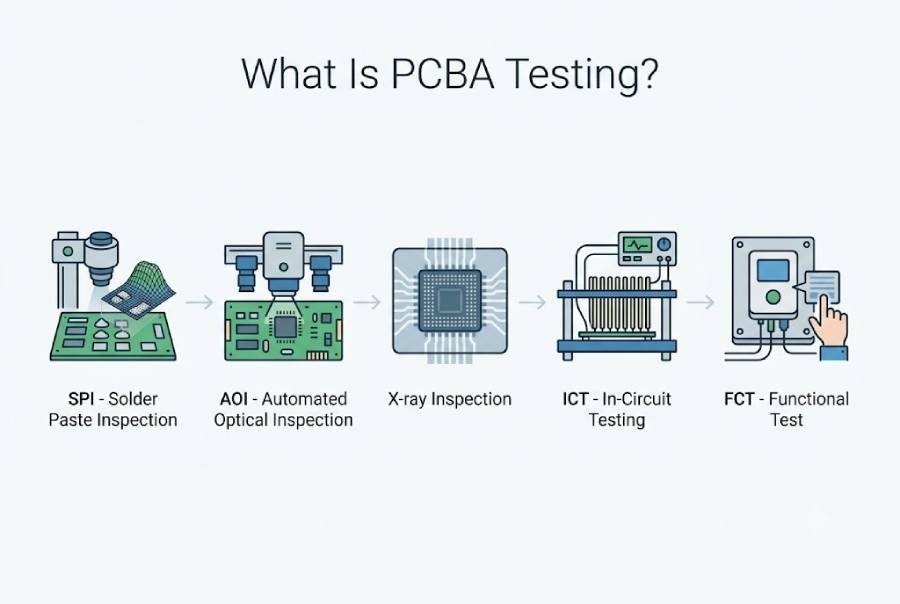
Typical Test Flow in a PCBA Line
In most factories, testing is not treated as one final step at the end of the line. Instead, verification is distributed across the assembly process so problems can be detected earlier, when they are cheaper and easier to fix.
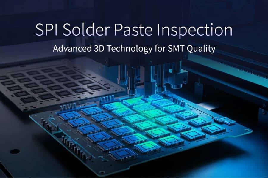
A typical workflow may begin with solder paste inspection, then continue through post-reflow AOI, X-ray for selected packages, ICT or flying probe, functional testing, and final visual or shipment inspection. This staged approach improves fault coverage because each method addresses a different failure mode.
To understand where testing fits in the wider production sequence, you can also review the main PCB assembly process steps, electronic PCB assembly process and flow chart, and SMT production line.
Test Coverage, Fixturing, and DFT Considerations
Test coverage is not the same across all methods. AOI is strong for visible defects, ICT and flying probe are better for electrical faults, and functional testing is better for real operating behavior. That is why a layered strategy usually performs better than relying on a single inspection step.
Coverage also depends on access. Even a strong electrical test method cannot perform well if test points are missing, blocked, or poorly planned in the layout. This is where DFT, or Design for Test, becomes important. Good DFT planning improves access to critical nets, reduces fixture complexity, and makes testing more reliable and scalable.
Fixture-based testing such as ICT usually requires higher upfront engineering and tooling investment, but it offers faster and more repeatable results at volume. Flying probe reduces that upfront burden, which makes it more attractive for low-volume or changing designs.
Common Failures Found by PCBA Testing
PCBA testing is used to identify the kinds of failures that can affect function, reliability, or long-term stability. These include soldering defects, component placement errors, polarity mistakes, electrical faults, and hidden structural issues inside the assembly.
Typical soldering defects include bridges, insufficient solder, excess solder, cold joints, and opens. Component-related issues may involve missing parts, rotated or skewed placement, incorrect polarity, or wrong-value passives. Hidden-joint problems under BGA or similar packages often require X-ray to detect, while functional testing may reveal startup problems, signal instability, or communication faults that are not obvious during visual inspection.
For related quality topics, you may also want to review common defects in lead-free PCB assembly and how to prevent them, quality checks for reliable through-hole PCB assembly, and BGA assembly soldering: overcoming challenges and ensuring quality.
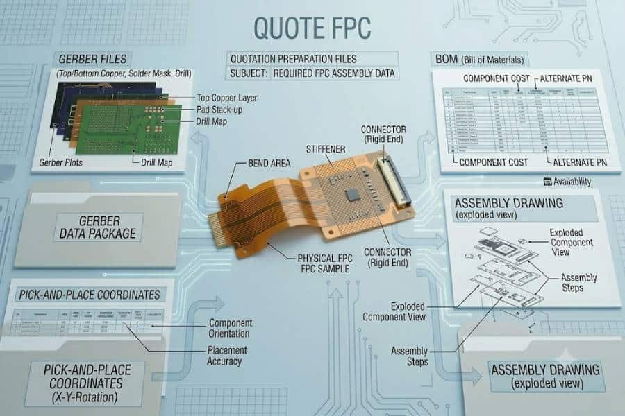
Preparing for Testing — What Customers Should Provide
Testing works much better when the customer provides a complete and accurate project package before production starts. Missing files or unclear requirements often delay engineering review and reduce the effectiveness of the planned inspection flow.
At a minimum, customers should usually provide BOM data, Gerber or ODB++ files, pick-and-place data, and assembly drawings. For stronger electrical and functional verification, it is also helpful to provide schematic files, netlist data, test-point information, firmware if required, and clear functional test expectations such as operating conditions and pass/fail criteria. A golden sample can also improve test setup and validation.
To prepare these materials more efficiently, see how to get a quote and order PCB assembly, what is the bill of materials.
Cost, Lead Time, and Policy Trade-Offs
Every PCBA test strategy is a balance between cost, speed, and risk control. More testing usually improves coverage, but it may also add fixture cost, programming effort, engineering time, and longer lead times.
For example, ICT often has a higher upfront cost because of fixture design and setup, but it becomes more efficient in stable, higher-volume production. Flying probe is more flexible and easier to launch, but it is slower per board and may not scale as well into larger programs. As a result, the best strategy is usually not the cheapest one or the most aggressive one, but the one that best fits the product and production stage.
For sourcing and planning decisions, this topic can also connect to SMT PCB assembly cost breakdown: what factors affect your project pricing, quick-turn PCB assembly in USA: the strategic guide to speed, cost, reliability, and how to choose the right quick-turn PCB assembly manufacturer.
FAQ
AOI checks visible assembly quality with cameras, while ICT checks the board electrically at the component and net level. AOI is better for placement and solder appearance, while ICT is better for shorts, opens, and wrong-value parts.
No. Functional testing verifies real operating behavior, while electrical testing such as ICT or flying probe focuses more on circuit correctness and component-level faults.
No. X-ray is mainly needed when the board includes hidden-joint packages such as BGA, QFN, or other bottom-terminated devices that cannot be evaluated fully through optical inspection alone.
Flying probe is often a strong choice for prototypes and low-volume runs because it avoids custom fixture cost and supports faster setup.
ICT is often the better choice for stable, high-volume production because it provides fast and repeatable electrical coverage once the fixture is ready.
Typical files include BOM, Gerber or ODB++ data, pick-and-place files, assembly drawings, and, when available, schematic, netlist, test-point data, firmware, and functional test requirements.
Conclusion
PCBA testing is one of the most important quality gates in electronics manufacturing because it connects assembly quality with real product reliability. By combining visual inspection, electrical verification, and functional testing, manufacturers can detect faults earlier, reduce rework, and lower the risk of field failure.
There is no universal test strategy for every board. The right approach depends on package type, production stage, required coverage, available documentation, and the business risk of failure. When DFT is considered early and the testing requirements are clearly defined, the entire assembly process becomes easier to control and more reliable to scale.